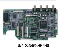
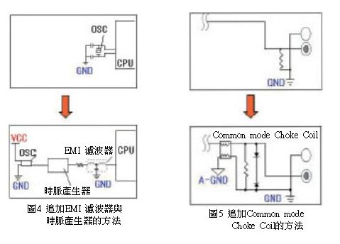
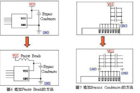
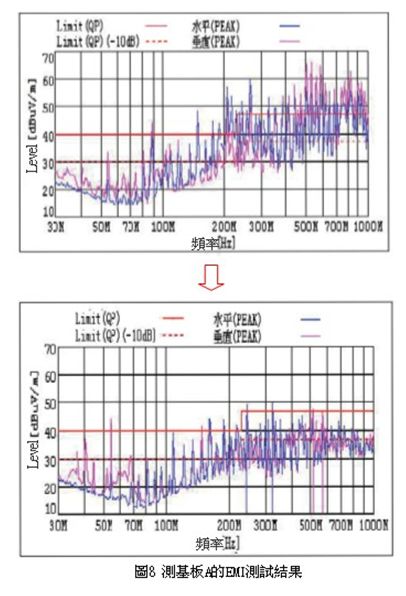
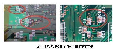
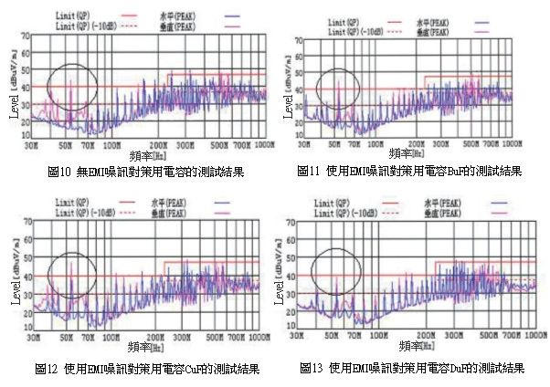
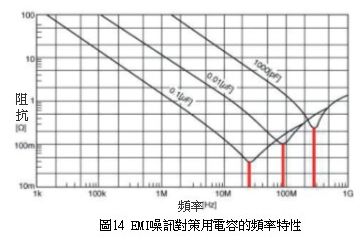
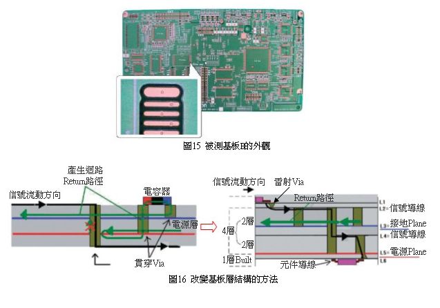
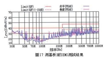
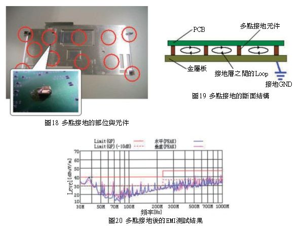
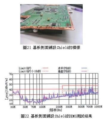
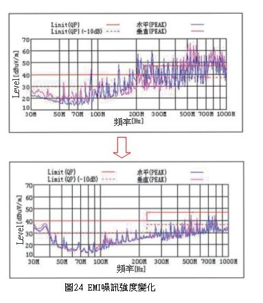
With the improvement of the functions of electronic components, various electronic products are constantly moving toward high speed. However, as a result of high performance, multi-functionality, and portability, various EMC (Electro Magnetic Compatibility) problems have become designers. A lingering nightmare. At present, EMI (ElectroMagnetic Interference) noise countermeasures mostly rely on the experience accumulated by designers for many years, or use simulation analysis software to analyze the frame structure and electronic components, and meet the requirements and specifications at home and abroad. In other words, electronic products have arrived. In the final evaluation and testing phase, we discovered and responded to EMI problems. After repeated review, re-testing and addition of countermeasure components, it often became the main reason for the expansion of design development time and the expansion of test costs. Test Conditions As shown in Figure 1, the test site is an indoor 3m semi-anechoic chamber, and the predetermined test frequency range is 30MHz~1000MHz. The peak point (Peak Point) is read as test data (Figure 2). 3 is an appearance of the substrate A to be tested. The substrate is a circuit board for an image processing system, and the operating frequency is 27 MHz and 54 MHz. The circuit board has a built-in CPU, Sub CPU, FRASH, and SDRAM×5, and image data/digital conversion processing. The unit and the image input/output unit are also in compliance with the requirements of "VCCI Specification Level B", and the same power board (Board) and transformer (Adapter) are used for the test. Add the Commonmode Choke Coil (DLWxxx series) to the image input/output unit (Fig. 5) Ferrite Beads (Fig. 6) is additionally added between the Bypass Condenser of each IC power input line and the power supply. Add the BypassCondenser so that all the power supply legs of each IC are powered from the base power layer (Plane) via the Bypass Condenser (Figure 7). Various EMI noise countermeasures a. EMI noise countermeasure capacitors Then, the EMI test is performed to obtain the test result of FIG. 8, and the noise suppression design operation is performed according to the test result. At the same time, the design data of the tested substrate A is read into the EMI noise suppression support tool, and the support tool is pointed out. The main parts, such as the frequency line and the Bus wire Via, are dispersed with EMI noise countermeasure capacitors (Fig. 9). The main reason is that if the return path of the signal wire is too long or discontinuous, the EMI noise increases. Oh, in order to shorten the Return path, set the capacitor that connects the power supply to the ground. 10 to FIG. 13 show the EMI noise test results when the capacitance is changed. According to the test results, the low-frequency noise level can be suppressed by the capacitance DuF for the large-capacity EMI noise countermeasure set in accordance with the frequency range of FIG. Although the capacitor is added to increase the capacity load of the PCB, in order to suppress noise, the capacitance frequency characteristics of each part are set, but the expected EMI noise suppression effect can be exerted. In practical applications, it is only necessary to disperse EMI noise countermeasures in the vicinity of the high-frequency conductor pattern such as the frequency conductor and the Bus conductor, in the vicinity of the internal plane (Plane) forming the CPU and the Return path, and in the vicinity of the side surface of the substrate on which the noise entrance and exit are formed. Capacitance can eliminate noise around the part. For a variety of substrate shapes, component packages, and lead PCBs, as long as the EMI noise countermeasure capacitors are provided at regular intervals, a dispersive noise suppression effect can be obtained. In practical applications, it is only necessary to disperse EMI noise countermeasures in the vicinity of the high-frequency conductor pattern such as the frequency conductor and the Bus conductor, in the vicinity of the internal plane (Plane) forming the CPU and the Return path, and in the vicinity of the side surface of the substrate on which the noise entrance and exit are formed. Capacitance can eliminate noise around the part. For a variety of substrate shapes, component packages, and lead PCBs, as long as the EMI noise countermeasure capacitors are provided at regular intervals, a dispersive noise suppression effect can be obtained. The main reason for changing the structure of the substrate to be tested is that the return path of the general 4-layer substrate is usually provided with a passable power source Plane or the shortest distance to the ground. Therefore, the return path is often caused in the penetration portion, if the signal wire is covered with the ground plane, Most of the Return path will flow into the ground Plane, which will solve the problem of the return path. The measured substrate B is made according to the above concept, so the Return path is reduced by 30% on the whole PCB, and the signal pattern and the Return path are reduced. The current loop distance, in turn, achieves the purpose of EMI noise suppression. Fig. 16 is a view showing the structure of each layer of the substrate B to be tested. 17 is an EMI noise test result of the substrate B to be tested. According to the test result, the field structure including the ground plane Plane using the outer layer and the design of the circuit bypassing the return path do have an effect of suppressing EMI noise, but actually Such a variety of circuit boards have to be changed in such a layer structure, which is bound to face the problem of increasing production costs. Especially when all signal wires are included in the design considerations, it is almost impossible to operate. Therefore, the Layout stage should avoid high frequencies. The signal conductors are routed through Via, and a ground plane must be placed in the layer adjacent to the signal conductors, thereby preventing the Return path from being detoured or broken. The ground planes are connected by a plurality of Vias, and the Return path is utilized by the complex Via for ideal return. return. c. Setting the multi-point Grand ground return current when flowing, the ground plane in the PCB will generate a potential difference, which is often one of the causes of EMI noise, and may form so-called secondary noise through the PCB, so The grounding Plane is connected to the metal plate at multiple points (Fig. 18, Fig. 19), so that the potential difference between the side and the center of the PCB is uniformized, and the impedance of the ground Plane itself is reduced (Impedance) and the voltage drop is suppressed. Figure 20 shows the EMI test results after multi-point grounding. It can be seen from the figure that the EMI noise intensity in the low-frequency domain is slightly increased, but the EMI noise is suppressed above 200 MHz, which means that the effectiveness of multi-point grounding is confirmed. d. Laying the Shield Figure 21 shows the actual appearance of the Shield on the side of the substrate. The specific method is to stick the conductive tape on the side of the substrate, in order to suppress the signal line inside the substrate, the noise of the Via and the power supply Plane, and then ground the outer layer. Plane connection, test the EMI noise shielding effect on the side of the substrate, Figure 22 shows the EMI test results of the Shield on the side of the substrate. According to the test results, the EMI noise intensity decreases below 200MHz, and even meets the specification level, confirming the side laying of the substrate. Shield does suppress EMI noise. When the actual PCB is fabricated, the Shield is laid on the side of the substrate, which also faces the challenge of rising cost. Similar to Figure 23, a new structure with ground Plane and continuity through Via near the side of the substrate, in addition to solving the cost problem, can effectively suppress the substrate. Side EMI noise intensity; Figure 24 is the PCB test result combined with the above various EMI noise countermeasures. Conclusion The EMI noise countermeasures introduced above are as follows: Set the capacitor for EMI noise countermeasures Avoiding the return of the return path of the substrate layer structure design Set multi-point Grand grounding Shield on the side of the substrate In fact, PCB EMI countermeasures will vary greatly with component packaging, wire, substrate shape, layer structure, and housing limitations. Therefore, this paper mainly discusses how to fully apply EMI noise countermeasures in the PCBLayout stage. A series of countermeasures to find the method that best meets the production cost while meeting the specification requirements. Accessories For Power Line Stringing
Accessories For Power Line Stringing Series of various types including Continuous Duct Rods,Fiberglass Duct Rods,Earth Drill,Earth Anchor,Pulling Socks,Joint Protector,Pole Climber,Wrenches,Conductor Spacer,Spacer Bike,Aluminum Ladder,etc,which is widely used in power line project.All of them are made of high quality materials with reasonable volume,light weight,easy to operate.By high quality material and good design,these kind of tools can be durable and long service life.we are a professional Chinese exporter of Electric Power Line Stringing Tools,and we are looking forward to your cooperation.
Yangzhou Qianyuan Electric Equipment Manufacturing & Trade Co. Ltd is specialized in manufacturing and trade of electric power line transmission tools. Our main products are Anti-twisting Steel Wire Rope,Stringing Pulley,Hydraulic Crimping Compressors,Engine Powered Winch,Motorised Winch,Wire Grip,Gin Pole,Cable Stand,Mesh Sock Grips,Cable Conveyor,Lever Chain Hoists and so on,which are mainly supplied to power companies,railroad companies and other industry fields.
Accessories For Power Line Stringing,fiberglass duct rodder,safety helmet,Joint Protector,pole climbers Yangzhou Qianyuan Electric Equipment Manufacturing & Trade Co.Ltd , https://www.qypowerline.com
One of the main sources of EMI, the printed circuit board (PCB), has been highly valued by designers since ancient times, especially in the PCB Layout stage. If EMI issues can be considered, it is usually possible. Effectively suppress the occurrence of noise in advance, in view of this article to explore how to fully apply the improvement techniques to suppress the intensity of EMI noise in the Layout phase of the PCB. 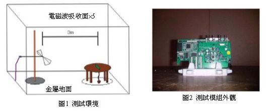
To assure the quality, we will do 100% inspection for raw material, production procedure, packing before shipment,
so we do have the confidence to supply customers with high-quality and high-efficiency products.
"Customer satisfaction" is our marketing purposes,so we have extensive experience in professional sales force,and strongly good pre-sale, after-sale service to clients. We can completely meet with customers' requirements and cooperate with each other perfectly to win the market.Sincerely welcome customers and friends throughout the world to our company,We strive hard to provide customer with high quality products and best service.