Abstract: In order to solve the data storage conflict of multiple ports accessing DDR3 in video graphics display system, an FPGA-based DDR3 storage management system is designed and implemented. The DDR3 memory control module uses MIG to generate DDR3 controllers, which can perform DDR3 read and write operations only through user interface signals. The DDR3 user interface arbitration control module divides the interrupt request into multiple sub-requests to implement parallel processing of video interrupts and graphics interrupts. The frame address control module ensures that the current output frame outputs the most recent full frame. The results show that the designed DDR3 storage management system simplifies the complexity of multi-port read and write DDR3 and improves the speed of parallel processing.
Introduction The on -board video graphics display system mainly realizes the drawing of 2D graphics, which constitutes various flight parameter pictures, and superimposes real-time external scene video. Because FPGA has powerful logic resources and rich IP core, FPGA-based embedded system architecture [1] is an ideal architecture choice for airborne video graphics display system. Video processing and graphics generation need to store a large amount of data, and the internal storage resources of the FPGA cannot meet the storage requirements, so external memory needs to be configured.
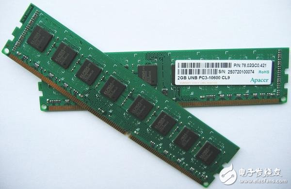
Compared with DDR2 SDRAM, DDR3 SDRAM has better bandwidth, faster transfer rate and more power saving [2][3], which can meet the requirements of large throughput and low power consumption. Therefore, DDR3 SDRAM is selected as the on-board video graphics display. The external memory of the system.
In this paper, Xilinx's Kintex-7 series XC7K410T FPGA chip and two Micron MT41J128M16 DDR3 SDRAM chips are used as hardware platforms to design and implement DDR3 multi-port storage management of FPGA-based video graphics display system.
1 Overall architecture designIn the on-board video graphics display system, in order to achieve multi-port read and write access to DDR3, the designed DDR3 storage management system is shown in Figure 1. It mainly includes DDR3 memory control module, DDR3 user interface arbitration control module and frame address control module.
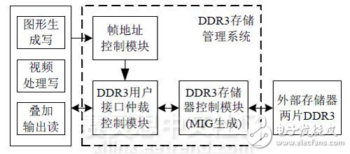
Figure 1 DDR3 storage management system design block diagram
The DDR3 memory control module uses Xilinx's MIG [4] (Memory Interface Generator) solution to establish the internal control logic of the FPGA to the DDR3 connection through the user interface. The user does not need to manage complex control logic such as DDR3 initialization and register configuration, and only needs to control. Read and write operations on the user interface.
The DDR3 user interface arbitration control module sets each data read and write request as an interrupt, and learns the arbitration control by borrowing the interrupt processing idea to solve the data storage conflict.
The frame address control module controls the switching of the frame address. In order to improve the speed of parallel processing and simplify data read and write conflicts, graphics data and video data are stored in different DDR3s.
2 DDR3 memory control module designThe logic block diagram of the DDR3 controller generated by MIG [5] is shown in Figure 2. The DDR3 read and write operations can be completed only through the user interface signal, which greatly simplifies the design complexity of DDR3.
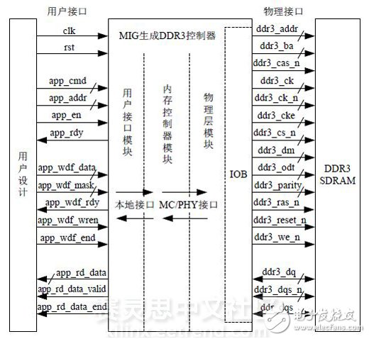
Figure 2 Logic block diagram of the DDR3 controller
2.1 DDR3 control module user interface write operation design
The DDR3 memory control module user interface write operation has two sets of systems, one is the address system, and the other is the data system. The user interface write operation signal description is shown in Table 1.
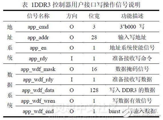
The contents of the address system are app_addr and app_cmd, which are aligned and bound. When app_cmd is 000, it is a write command. When app_rdy (DDR3 control) and app_en (user control) are simultaneously raised, app_addr and app_cmd are written to the corresponding FIFO. The content of the data system is app_wdf_data, which stores write data to the write FIFO when both app_wdf_rdy (DDR3 control) and app_wdf_wren (user control) are pulled high.
In order to simplify the design, the user interface write operation timing designed in this paper is shown in Figure 3, so that the two systems are completely aligned in timing.
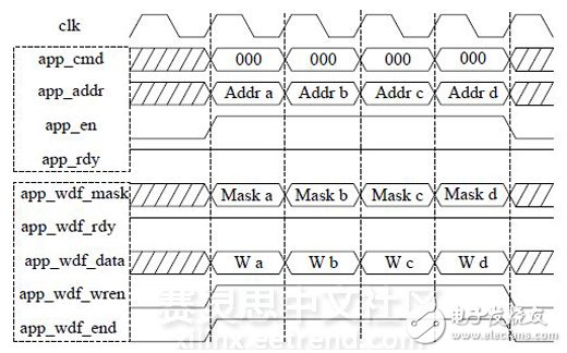
Figure 3 DDR3 write operation timing diagram (burst length BL = 8)
2.2 DDR3 Control Module User Interface Read Operation Design User interface read operations are also divided into address system and data system. The user interface read operation signal description is shown in Table 2.
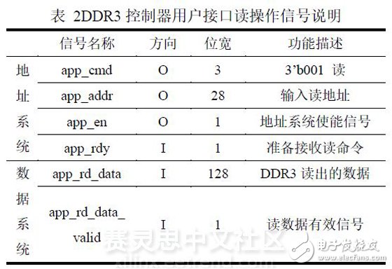
The address system is the same as the write operation. On the rising edge of the clock and when app_rdy is high, the user port simultaneously issues a read command (app_cmd=001) and a read address, and pulls app_en high, writing the read command and address to the FIFO. For the data system, when app_rd_data_valid is valid, the read data is valid, and the read data sequence is the same as the address/control bus request command.
The read operation address system and data system are generally not aligned. Because the address system sends to DDR3, DDR3 requires a certain reaction time. The read operation timing is shown in Figure 4.
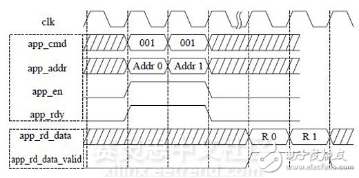
Figure 4 DDR3 read operation timing diagram (burst length BL = 8)
Pv Branch Connector,Mc4 Y Type Connector,Mc4 Branch,Mc4 Branch Adapter
Sowell Electric CO., LTD. , https://www.sowellsolar.com