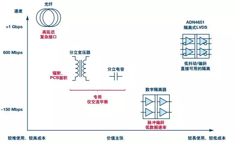
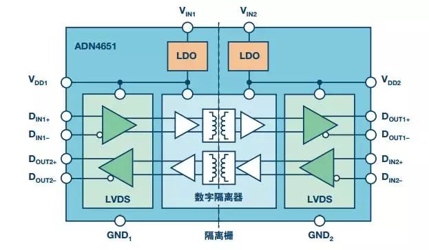
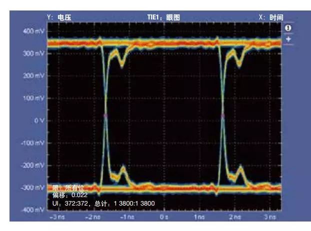
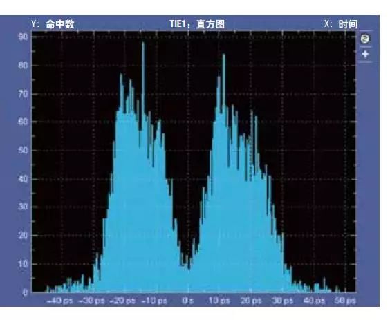
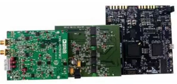
External interfaces in harsh environments need to be galvanically isolated to enhance safety, functionality, or immunity. This includes the analog front end in the data acquisition module used for industrial measurement and control, and the digital interface between the processing nodes. Low Voltage Differential Signaling (LVDS) is a high speed interface commonly used in higher performance converters and high bandwidth FPGAs or ASCIs. Differential signal transmission is highly resistant to external electromagnetic interference (EMI) (due to the mutual coupling between the inverting and in-phase signals), and correspondingly minimizes any EMI due to LVDS signal transmission. . Adding isolation to the LVDS interface is a transparent solution that can be plugged into existing signal chains for high-speed and precision measurement and control applications. What options are there today? For galvanic isolation of converters and processor interfaces , standard digital isolators are a much faster, robust, and more reliable solution than optocouplers. However, typical LVDS data rates that support high-speed or precision converters are hundreds of Mbps, but the fastest standard digital isolators support up to 150 Mbps. To support higher bandwidth isolation, system designers have now turned to custom design-intensive solutions such as deserialization or separation schemes using transformers and capacitors. These solutions add cost and design time, and the deserialization scheme may even require the addition of a simple set of FPGAs for the purpose of isolation. Transformers and capacitors require careful signal conditioning of the LVDS signals, and the resulting application and data rate specific solutions will require AC balanced coding. A further solution is to use fiber optic communication links, but this is more suitable for the needs of several Gbs due to cost and higher complexity. Figure 1 shows the various options for high-speed isolation, drawn in terms of value proposition (depending on design difficulty and cost) relative to the maximum speed of the solution. Figure 1. The relationship between the value proposition of the isolator implementation and the isolator speed As a comparison (shown in Figure 2), Analog Devices has introduced a range of directly available LVDS isolators: the ADN4650/ADN4651/ADN4652, which are enhanced with iCoupler® technology for speeds up to 600Mbps. Figure 2. ADN4651600 Mbps LVDS Isolator Block Diagram In addition to the TIA/EIA-644-ALVDS-compatible I/O, its complete isolator signal chain is fully differential, enabling high noise immunity and low-radiation solutions. It provides two isolated LVDS channels, one for one reception (ADN4651, opposite ADN4652), or two for transmission or reception (ADN4650). The internal high-speed circuit operates at 2.5 V and may not be available in industrial systems, so it has a low-dropout regulator (LDO) as shown in Figure 3 to support a single wide-body SOIC solution, even with a 3.3 V supply. It doesn't matter. Are these new LVDS isolators a directly available solution? To ensure that these LVDS isolators can be plugged into the converter's interface, or in an interprocessor link running at up to 600 Mbps, the ADN465x family has ultra-low jitter precision timing. This is important because at 600 Mbps, the unit interval (UI, such as bit time) is only 1.6 ns, so the jitter on the edges must be very small so that the receiving device has enough time to sample the bits. The typical total jitter of the ADN465x is 70 ps, ​​or less than 5% UI at 600 Mbps, assuming a bit error rate of 1 x 10-12. How to quantify jitter? The most basic way to view jitter is to use a differential probe to measure the LVDS signal pair, and both the rising and falling edges are triggered, and the oscilloscope is set to infinitely continuous. This means that the high to low and low to high transition will be superimposed to each other, the crossover point can be measured. The crossover width corresponds to the peak-to-peak jitter or the time interval error (TIE) measured so far (compare the eye and histograms shown in Figure 3). Some jitter is caused by a random source (like thermal noise). This random jitter (RJ) means that the peak-to-peak jitter seen on the oscilloscope is limited by the run time; as the run time increases, the tail on the histogram Will rise. Figure 3a. Eye diagram of the ADN4651 Figure 3b. Histogram of the ADN4651 In contrast, sources of deterministic jitter (DJ) are bounded, such as jitter caused by pulse skew, data rate dependent jitter (DDJ), and inter-symbol interference (ISI). Pulse skew originates from the difference between high to low and low to high propagation delay. This can be visualized by offset crossover, ie at 0 V, the two edges are separated (it is easy to see through the separation in the histogram in Figure 3). DDJ is derived from the difference in propagation delay at different operating frequencies, while ISI is derived from the effect of the previous transition frequency on the current transition (edge ​​timing is usually different after a series of 1 or 0 seconds and 1010 mode codes). In order to fully estimate the total jitter (TJ@BER) at a particular bit error rate, RJ and DJ can be calculated from the model to which the measured TIE distribution fits. One such model is the Double Dirac model, which assumes that the Gaussian random distribution is convolved with the Double Dirac δ function (the separation distance between the two Dirac δ functions corresponds to deterministic jitter). For a TIE distribution with significant deterministic jitter, the distribution is visually similar to this model. One difficulty is that certain deterministic jitters have an effect on the Gaussian component, ie the double Dirac function may underestimate deterministic jitter and overestimate random jitter. However, the combination of the two still accurately estimates the total jitter at a particular bit error rate. RJ is defined as the 1 σ rms value in the Gaussian distribution model. To infer a longer run length (low BER), simply select the appropriate multi-σ to move it a long enough distance along the end of the distribution (1× A 10-12 bit error requires 14 σ). The DJ is then added to provide an estimate of TJ@BER. Signals for a plurality of chain elements, a plurality of lead and its increase in jitter TJ overestimated values, as the value of the geometric sum RJ, DJ the algebraic sum value, which would provide for a more complete signal chain Estimated for a reasonable complete TJ@BER. The RJ, DJ, and TJ@BER of the ADN4651 are all specified separately, providing maximum values ​​based on statistical analysis of multiple units to ensure that these jitter values ​​are maintained over power, temperature, and process variations. How do different LVDS interfaces rely on precision data transitions? A typical receiver can tolerate 10% to 20% UI jitter. For example, isolating an external LVDS port with the ADN465x will allow the industrial backplane to safely extend over the cable between the PLC and the I/O module. The maximum cable distance depends on the allowable data rate, cable structure, and connector type, but at lower data rates (for example, 200 Mbps) and when using high-speed connectors and appropriate shielded twisted pairs, the cable length is several meters. Possible to achieve. The ADC interface typically uses LVDS for source synchronous data transmission. This means that the LVDS clock will be sent in parallel with one or more data bitstreams on other LVDS channels. The low channel-to-device and inter-device skew of the ADN4650 (≤300 ps and ≤500 ps, ​​respectively) is beneficial. These skew values ​​account for the largest difference between high to low (or low to high) propagation delays across multiple channels, and statistically guarantee the performance of all ADN4650 devices over power, temperature, and process variations. Data transfer is performed on both the rising and falling clock edges to achieve double data rate (DDR) (some converters use DDR to increase the output bandwidth), and low pulse skew of ≤100 ps supports clock synchronization. The ADC sample clock may need to be isolated to successfully isolate the analog front end using an external clock source; for example, to simultaneously provide a clock signal for a set of multiple data acquisition channels. This is a challenge for any isolator because any jitter on the clock is directly added to the aperture jitter, which in turn reduces the quality of the measurement. At the same time, like clock sources, devices used for clock distribution in the LVDS signal chain, such as fan-out buffers, typically specify this jitter as additive phase jitter. This means that the phase noise of the input clock is compared to the phase noise of the output clock and the difference is integrated over the relevant frequency range (typically 12 kHz to 20 MHz). The ADN465x family is essentially an LVDS buffer with integrated isolation, so the same argument applies to the analysis of the effects on ADC sampling. When using the ADN465x, ensure that the typical additive phase jitter is only 376 fs, which maintains the original measurement quality even with increased galvanic isolation, because adding isolation eliminates noise in the processor-side digital circuitry. 600 Mbps error-free transmission, 300 MHz clock synchronization, and maximum ADC performance and resolution with the sample clock isolated are already referenced by the AD7960 (18-bit, 5 MSPS, SAR ADC) in reference circuit CN-0388 Verification, as shown in Figure 4. Figure 4. ADN4651 isolation circuit for the AD7960 and SDP-H1 The existing ADC evaluation platform between the ADC board and the high-speed SDP-H1 evaluation platform is isolated using a riser card that transparently isolates the analog front end. The software has not changed, and the evaluation of the data sheet specifications using a sophisticated analog signal source confirms that it has the same performance as a non-isolated platform. What other applications can be isolated using LVDS? Isolated analog front ends or isolated industrial backplanes are two useful application examples that showcase the opportunities offered by LVDS isolation, but there are many other applications for this technology. Video signals sent to flat panel displays typically use LVDS signals, while HDMI® signals use similar differential signal common mode logic (CML). These typically do not require isolation, but for applications such as medical imaging or external display ports in industrial PCs, galvanic isolation can protect the human body or equipment. Connecting Terminals,Micro Connecting Terminal,Aluminum Connecting Terminals,Connecting Copper Terminal Taixing Longyi Terminals Co.,Ltd. , https://www.longyicopperlugs.com