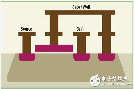
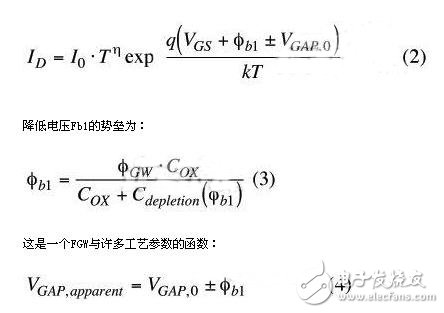
The cost of a transponder design depends on several factors, not just the cost of silicon. In fact, the cost of the chip manufacturing process (in terms of complexity and maturity and yield) can generally be controlled by the circuit designer. According to experience, when the die area exceeds 1 mm2, the cost of RFID for supply chain applications begins to decline. When the RFID transponder moves from the minimum range of the system to the maximum range, its power roughly changes by a factor of thirty, so the power requirements of the RFID transponder may present a difficult challenge for the designer. Although the typical power available to UHF RFID transponders is on the order of one hundred milliwatts, the problem is not limited to power consumption. Even within short distances, enough power can be supplied to the transponder but it can cause voltage overload. The transponder must also operate from a nominal operating range of -25°C to +40°C and an extended temperature range of -40°C to +65°C based on the EPCGen2 standard. Cost and power requirements greatly influence the choice of process for producing RFID transponder ICs. As mentioned in the previous series, Schottky contacts provide low turn-on voltage, low junction capacitance, and high current drive in RFID transponder designs. In addition, there have been efforts to adopt new processes such as BiCMOS and sapphire wafer (SOS), which provide excellent low power performance. But each method has its downside. Schottky contact is not conventional in CMOS processes and generally requires post-processing steps. Other processes such as BiCMOS and SOS are too expensive for most RFID transponder applications. Another method to achieve low power circuit requirements is Dynamic Threshold Voltage MOSFET (DTMOS) technology. It can achieve low-cost production using bulk silicon CMOS technology. All of its advantages are ideal for developing the next generation of UHF RFID transponders, which are discussed in more detail in this article. This article will first introduce the basic principles of DTMOS. Next, the implementation of DTMOS in the digital, analog, and RF fields will be highlighted, as UHF RFID transponders include circuits in all three areas. Finally, a chip implementation of the DTMOS bandgap reference circuit that satisfies the EPCGen2 specification UHF RFID will be demonstrated. DTMOS is a MOS transistor that basically uses interconnected wells and gates (Figure 1). For the dual-well p-substrate CMOS process, P-type DTMOS can only be used because of the fact that the N-well can only be controlled and produced separately, because the P-well of the N-type DTMOS has a common and low ohmic to the P substrate. Pathway. However, N-type DTMOS can be obtained in a process having deep N-well characteristics. The operation of DTMOS is similar to the operation of a weak inversion MOS, similar to triode operation in a lateral PNP tube. The leakage current of the weak inversion MOS transistor and the collector current of the lateral PNP (both in the saturation region) are: Where: F = FBJT = VBE. For the triode, F=FWIM=[(VGS-VT)&TImes;COX/(COX+CdepleTIon)] for weak inversion MOS transistors. The value of the depletion layer capacitance depends on the width of the depletion layer, which in turn depends on the doping characteristics of the well and the voltage drop near the source junction in silicon. Therefore, this factor depends on the well-source voltage employed and the well-source voltage used by the threshold modulation effect. The DTMOS can be viewed as a lateral bipolar PNP tube with an extra gate on the base. Based on this view, the leakage current of DTMOS mainly depends on the voltage passing through the source-well junction, which produces an ideal exponential (similar bipolar) relationship between VGS and ID. Due to the presence of the interconnect gate-well, there is a built-in voltage FGW between the gate and the well. Due to the distribution of the capacitance, the voltage FGW is redistributed on the gate oxide and silicon. This means that the voltage drop in silicon is reduced by the FGW as a barrier, and the leakage current of DTMOS can be expressed as: The key results from these derivations are as follows: 1. Compared with the 1.2V of the silicon PN junction, the band gap of the DTMOS device is obviously 0.6V; 2. DTMOS devices have ideal exponential characteristics [IDaexp(qVGS/kT)]; 3. The lateral current of the DTMOS device has an exp(qFb1/kT) factor which is larger than the usual lateral PNP; 4. The bandgap voltage has a significant temperature dependence. The initial successful design using the 0.25um DTMOS process was performed at 77K, using a 0.6V supply voltage and connecting the substrate to a fixed forward bias voltage. Subsequent experiments included a controlled gate lateral bipolar transistor (GCLPNP) and a silicon-on-insulator (SOI) MOSFET process with the substrate connected to the gate terminal. The first process is used for small, low-power analog applications, while the second is the best candidate for ultra-low-power CMOS. DTMOS technology offers amazing performance advantages over traditional CMOS technology in terms of its resulting gate-delay/power consumption. DTMOS also shows superior performance in RF circuits. In conventional CMOS, the process of shrinking to smaller feature sizes and threshold voltages (VTH) increases the speed of operation. However, the reduction in VTH also leads to a decrease in the behavior of subthreshold MOSFETs. The increase in quiescent current in the static circuit limits the VTH to 0.4V. DTMOS may be able to overcome these constraints, especially at very low VDD and low VTH with steep subthreshold characteristics. For DTMOS, the gate input voltage is forward biased to the substrate, and according to the well-known body effect formula, VTH will be reduced:
12v power supply is suitable for LED, Electronic cigarette, Tablet, Water purifier, Router, CCTV camera, LCD, Motor, Fan, Toys Medical machine, POS machine, Beauty & Health equipment, Humidifier, LED lights etc.
We can meet your specific requirement of the products, like label design. The plug type is US/UK/AU/EU. The material of this product is PC+ABS. All condition of our product is 100% brand new. You can send more details of this product, so that we can offer best service to you!
12V Power Supply,12V Pc Power Supply,12V Dc Power Supply ,12V Power Supply For Pc Shenzhen Waweis Technology Co., Ltd. , https://www.waweispowerasdapter.com


