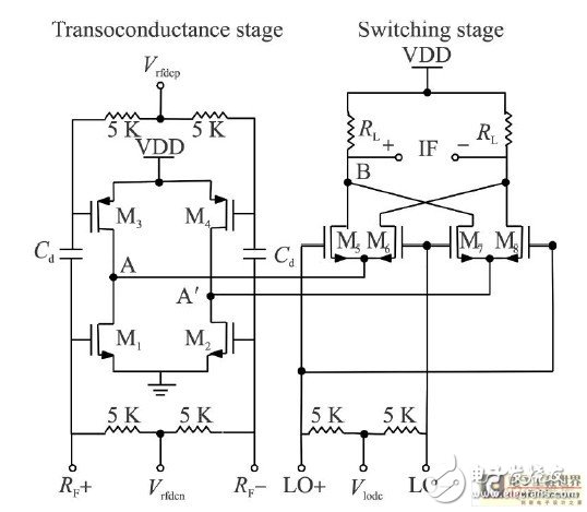
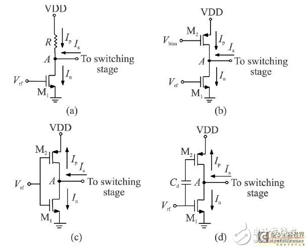
Currently, wireless communication devices are moving toward low voltage, low power consumption, low noise, and high linearity. As one of the key modules in the transceiver, the mixer has a direct impact on the above performance of the communication device. With the development of microelectronics technology, the gate length of CMOS devices is further reduced, and the overdrive voltage of MOS devices is further reduced, which makes it possible to design low-voltage and low-power RF circuits, but reduces the gate length of MOS devices. Lowering the operating voltage is limited. Therefore, circuit designers have focused more attention on circuit topologies, making RF circuits with low-voltage structures a hot topic. The traditional Gilbert mixer is composed of a transconductance stage, a switching stage, and a load stage stack, and its structure is a transconductance stage, a switching stage, and a load stage from bottom to top. In this configuration, all DC current flows through the transconductance stage, the switching stage, and the load stage. The transconductance stage and the switching stage circuit both require a turn-on voltage (VON), and the load stage also has a certain voltage drop (VRL). Therefore, the minimum value of the power supply voltage is Vdd,min = 2Von +VRL. If a low supply voltage is used, this configuration does not guarantee that all of the tubes are operating in the saturation region. That is to say, the Gilbert mixer can not meet the requirements of low voltage, and needs to be improved. For example, the literature [2 - 3] proposes to eliminate the tail current tube to reduce the power supply voltage. The literature [4 - 11] uses folding The structure replaces the stacked structure to solve the above problem. The literature [8] gives a comparison of the folded structure and the stacked structure. The folded structure adds two RF interrupt circuits and a coupling capacitor. In this way, for the DC channel, the transconductance stage is separated from the DC circuit of the switching stage and the load stage, and the two branches are independent of each other and do not affect each other. The supply voltage only needs to provide a value equivalent to a turn-on voltage (Von) to allow both the cross-catheter and the switch to operate in their respective saturation regions, ie the minimum supply voltage Vdd,min = Von + VRL. A low supply voltage is achieved. However, RF interrupt circuits are typically implemented using an LC resonant network, and the use of inductors increases the layout area and noise of the circuit. In this paper, a new folded structure mixer is designed. The circuit does not use an LC resonant circuit with a large inductance. When operating at 1.2 V, low voltage, low power consumption, low noise and high linearity are obtained. . The folded mixer topology designed in this paper is shown in Figure 1. M1 to M4 are transconductance stages, M5 to M8 are switching stages, and RL is the load resistance. The RF input is connected to the matching network, and the IF output is connected to the source follower as an output buffer (buffer). Figure 1 AC-coupled folding mixer topology The transconductance stage of the folding mixer circuit adopts current multiplexing technology, and the NMOS tube (M1, M2), the PMOS tube (M3, M4) and the DC blocking capacitor Cd constitute an AC-coupled complementary transconductance structure. The output of the transconductance stage (points A, A') is connected to the source of the switching transistor. The transconductance stage is directly connected to the supply voltage, so that the DC current across the conduits M1 and M2 consists of two parts, one from M3 and M4 and the other from the switching tube and load resistor, achieving the goal of low supply voltage. Since the current flowing through the switching stage and the load stage is small, on the one hand, the flicker noise generated by the switching tube is reduced, and on the other hand, the load resistance RL value can be appropriately increased, thereby increasing the conversion gain of the mixer. Therefore, the circuit not only satisfies the requirements of low voltage, but also ensures that the mixer has good performance under low power supply voltage. Figure 2 shows several folding mixer transconductance circuits. Figure 2 (a) In the transconductance stage NMOS transistor M1, the drain terminal is connected to the load resistor R. The current In of the M1 tube is shunted at point A, one part flows through the switch tube (Is), and the other part flows through the load resistor (IR), but this A disadvantage of the transconductance circuit is that a portion of the RF signal is leaked to the AC ground through the load resistor R. In order to reduce the loss of the RF signal, it is necessary to increase the resistance R, which in turn reduces the DC voltage of the node A. Under the low power supply voltage, the M1 tube cannot be guaranteed to operate in the saturation region. To solve this problem, replace the load resistor R with an active load, as shown in Figure 2 (b). However, the PMOS transistor here only increases the impedance between the node A and the power supply voltage. If the gates of M1 and M2 are connected to form a CMOS inverter structure, then M2 can increase the impedance and can also be shared with M1. Amplify the RF signal, as shown in Figure 2 (c), thus completely avoiding the RF signal leaking through the M2 to the AC ground. As can be seen from the figure, Is =In + Ip , total transconductance gm = gm n + gm p (gm n is the transconductance of the NMOS transistor, gm p is the transconductance of the PMOS transistor), so the CMOS inverter effectively improves the mixing The conversion gain of the frequency converter. Figure 2 Several structures of the transconductance stage of the folding mixer Then analyze the DC operating condition of the structure. The gates of M1 and M2 are added with the same bias voltage Vrfdc. Assuming Vt is the threshold voltage of the MOS transistor, Vovn is the overdrive voltage of M1, and Vovp is the overdrive voltage of M2. : Vovn =Vrfdc - Vt , Vovp =Vdd - Vrfdc -Vt , so the minimum supply voltage is Vdd,min = Vovn + Vovp + 2Vt. Spring Clamp Terminal Block,Screwless Spring Terminal Blocks,Spring Conductor Terminal,Spring Clip Terminal Blocks Wonke Electric CO.,Ltd. , https://www.wkdq-electric.com
