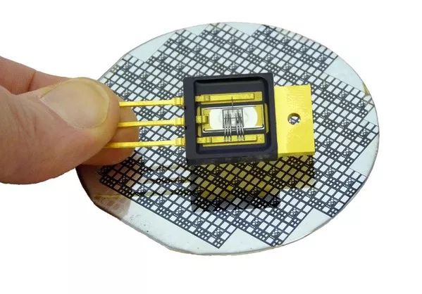
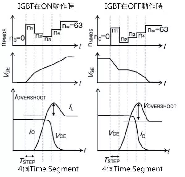
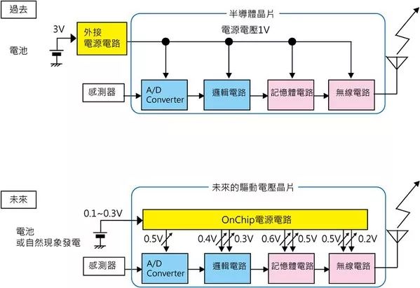
For wearable products such as smart watches and IoT devices, achieving low power consumption goals in the power sector, eliminating the need for frequent annoying charging actions, and ensuring adequate power supply when used as desired, is related to product trustworthiness and The key issue of value . For the moment, whether it is vibration, temperature difference, solar energy, power generation technology that utilizes natural phenomena, although it is possible to replenish the required power in time, it is expected that the wearable product or the Internet of Things device will not suddenly have a power interruption at an important moment . Power management design becomes relatively important when it comes to fatal problems . Many power supply circuits, electronic circuits, rechargeable batteries, and household AC power supplies are all developed on the premise of providing stable power output to provide required power, due to the power generation technology using natural phenomena as described above. Because it is very unstable power at a relatively low voltage, the corresponding power supply technology is necessary. In general, AC-DC converters, DC-DC converters, inverters, etc. are all powered by power control circuits, power supply components (IGBTs and power MOSFETs, etc.), gate drivers (Gate Drivers), and isolators ( Isolator) and so on. However, in the current power semiconductors, it is a new generation of power sources such as SiC (silicon carbide) and GaN (gallium nitride). The components are quite high-profile . By using these power semiconductors, not only can higher power conversion efficiency be achieved, but also small size and light weight can be achieved. In fact, industrial equipment, vehicles, and green energy equipment have begun to be applied, and the power supply has been improved in efficiency and miniaturization. On the other hand, it can also feel that the existing silicon power semiconductors are gradually at a disadvantage, but it is not very appropriate to simply switch to a new generation of power components simply because of this. Recently, the appearance of insulated gate bipolar transistors (IGBTs) has been significantly improved. Due to the improvement of the internal structure and the neglect of the process, it can be felt that the power waste has been reduced and the conversion efficiency is obvious. The result of the improvement. Figure 1: Higher efficiency pursues SiC (silicon carbide), GaN (gallium nitride) will become the mainstream component of next-generation power supply Therefore, with the advanced structure design and process technology, after improving the silicon power semiconductor of IGBT and the like, in order to pursue higher efficiency, it is not only possible to abandon the silicon power semiconductor component and change to SiC (silicon carbide), GaN. A new generation of power components such as (GaN). In addition, the gate driver (Gate Driver) is composed of an amplifier circuit (Amplifier) ​​and a transistor switch (Switching transistor), and then the gate of the IGBT is connected to the output of the gate drive, and then the drive signal is transmitted. To control the on or off of the IGBT, the most important of which is the waveform of the drive signal . For the stability of the waveform, it directly affects the conversion efficiency (power consumption) of the power supply and whether the noise is too large . For example, if the waveform rises sharply due to the enhanced conversion efficiency, the current waveform will have an instantaneous overshoot to increase the noise. Therefore, at this time, in general, the power supply designer will increase the resistance in the circuit connecting the IGBT and the gate driver to adjust the conversion efficiency and the trade-off of the noise, but the parameters can be adjusted only for the impedance. Values, only a few cases have the opportunity to achieve efficiency adjustments. The waveform of the drive signal output from the Gate Driver can be digitally programmable, so that the waveform can be arbitrarily set. For example, with 4 or 8 Time Segments, an independent 64-step adjustable voltage is provided for each Time Segment. When the initial Time Segment suddenly sets a high voltage, it can achieve a fast rising drive signal. Conversely, after the initial low voltage is set, the voltage value added in the Time Segment will slowly rise. The setting flexibility of such a driving signal waveform is quite high. If there are 4 Time Segments, there are 64 times multiplied by 4 Time Segments, and a total of 16.77 million combinations can find the best under limited human resources. Waveform. Figure 2: Using the digitally programmable waveform of the output drive signal, you can freely set the fineness of the waveform. In the current application market, the equipment and products that can be connected to the network are rapidly increasing in sales of new-type products every year. On the other hand, the development trend of this type of products is becoming more and more compact and portable. . It's like a portable medical device, including common measuring sensors, and then evolved into a body-mounted heart rhythm adjuster or artificial inner ear hearing aid. As long as the type of product placed on the body has wireless function, Ability to automatically connect to the network. However, whether these products are wearable or can be buried in the body, and the so-called IoT products have the same research and development topic, that is, how to stably supply the driving power required by the products . The comfort of these wearable products will directly affect the desire to buy, so in appearance, it is often designed to be light and thin, or rely on adding more types of sensors to achieve the purpose of humanization. However, for this purpose, the battery capacity of the power supply will be limited to a certain range, or it is designed so that the user cannot replace it, so it is necessary to attach an annoying charging power cord if it is impossible. Effective power consumption management will inevitably require the user to perform charging after a period of time. For example, products such as prosthetic devices that can be connected to the Internet, if there is no interruption in the ongoing networking operation, and there is insufficient power, then the charging power cord needs to be connected, but the general power cord is in use, such as the length or the turning point. , will cause a certain degree of discomfort to the user. Therefore, when using an IoT terminal that cannot replace the battery by itself for a long time, the low voltage and low power consumption technology of the semiconductor component is very important . In particular, semiconductor component driving technology using a low-voltage power supply of 1 V or less, and products that generate electricity using natural phenomena. At present, the power supply voltage of a 1.2V voltage-driven CMOS circuit is mostly reduced to 0.3V, although the power consumption can be reduced to 1/1000, but the response speed is also 100 times slower. As a result, although the efficiency of energy has increased by 10 times, it also affects the performance of the product. However, due to the influence of low voltage, the reaction speed is slow. In this respect, it may be considered to use time-sharing or multi-core to compensate for the basic structure of low voltage. Of course, we also know that we can't simply reduce the voltage, because the current semiconductor chips, in addition to logic circuits, continue to add component circuits, including memory, AC-DC transformers, wireless circuits, etc. These can drive all functional circuit blocks with a 1V supply voltage. However, when the driving voltage drops to 0.5V, the various functional circuits built into the chip will change to different degrees, so that the voltage that satisfies the various functional circuit blocks can be provided. Indispensable considerations and work, when faced with various voltage requirements, multi-voltage power supply has become one of the necessary capabilities of a single chip. Figure 3: Providing voltages for various functional circuit blocks is an indispensable consideration and work for future development For example, if 10 different voltage power supplies are required in a single chip, it may be necessary to prepare 10 different external power supplies, which is quite inconvenient for the user, which promotes single-chip multi-power circuit. And low-power technology development, like the fourth generation of Intel's Core architecture Haswell (development code), using 13 different power supply voltages inside its single chip. The use of natural phenomena power generation technology must consider the conditions of extremely unstable voltage input. In the case of IoT products that use natural phenomena power generation technology, in the power supply circuit, it is necessary to consider the conditions of extremely unstable voltage input. At this point, the boost circuit becomes very important. For example, in a product that uses a temperature difference between room temperature and room temperature to generate electricity or solar power, the output voltage of the power generation is about 100 mA or less. If you need to operate a component with a driving voltage of 1 V, you must rely on powerful. Boost circuit. For such a demand, the power chip manufacturers on the market provide corresponding products, for example, can support 20mV boost power components, but in order to complete the overall power circuit structure, it is also necessary to consider the use of a 1 to 100 transformer and other external Additional components are used to achieve IoT products that allow users to use wearables and the like without worrying about power problems. In fact, for the case where the supply voltage is 100mV, there is a certain degree of technical difficulty. According to the actual design experience, in the case of boosting at 80 mV, the MOS transistor cannot be used for switching operation in the booster circuit, and the voltage of 80 mV is much lower than the operating threshold voltage of the MOS, so there is no way. It is also very important that the gate input is in the ON state, so inside the chip, it is necessary to raise the gate voltage to achieve the gate actuation. At this time, the charge pump can be used. In the charge pump converter that accepts 80mV, since the driving force is still very low, the charge will be stored bit by bit, from 0V to 0.5V. Slowly boost, when stored to a certain amount of energy, send 0.5V of power in one breath, forcing the switch (ON / OFF) action, and if further, can also remove the inductor on the single-chip variable piezoelectric path Component. In addition to the voltage problem, there are various problems to be solved in order to stabilize the power supply under natural power generation. For example, when RF wireless charging is used, the generated microwave radiation also affects the power variation. And these RF wireless charging are almost all high frequency waves from above 1 GHz. The same voltage obtained by RF wireless charging is also quite low. At this time, how to perfect the high-frequency low-voltage boosting technology is also very important. In addition, when using piezoelectric components to generate electricity, it will also face an AC voltage of 30V. At this time, it is necessary to consider how to effectively control the high-voltage AC. As the functionality and charging capabilities of IoT products continue to increase, the internal semiconductor components will become more and more complex, and the division of labor will become more and more fine. At this time, how to reduce production under mass production The difficult problem of cost is that when power is supplied by different natural phenomena, it is necessary to match different power processing units and circuits. Of course, it is also possible to use the same power processing unit and circuit. By adjusting the characteristics of the input, it can meet different power supply sources. Although it solves the problem of the cost of matching one power supply to one power supply, it can still be achieved. The purpose of power optimization. Based on such a concept, in fact, some experts have conducted related research, but in the end, they all ended up with abandonment, and the reason is that efficiency cannot be optimized. Perhaps the same power supply circuit to match the concept of various power supply ideas, or must wait for future power component manufacturers to develop smarter, more efficient new products.
Blue light filter-using blue light filter technology can eliminate blue light on the phone screen, thereby reducing eye fatigue and fatigue. And keep your eyes healthy and avoid staring at the screen.
Ultra-transparent and protective Ultra-high-quality Ultra HD provides you with clear viewing effects. Let you fully enjoy the super retina display of the screen.
Evacuation Waterproof and Waterproof-The hydrophobic and loose oil transparent layer is used as the final coating to protect screen fingerprints, liquid residues and other stains, keeping your phone in its original condition all day long.
The 0.14mm high-sensitivity touch Ultra-Thin Protective Film can provide real touch and high sensitivity, ensuring that the original high-response touch is not disturbed.
If you want to know more about Anti-Blue Light Screen Protector products, please click the product details to view the parameters, models, pictures, prices and other information about Anti-Blue Light Screen Protector.
Whether you are a group or an individual, we will try our best to provide you with accurate and comprehensive information about the Anti-Blue Light Screen Protector!
Anti-blue Screen Protector, Anti-blue Light Protective Film, Anti-blue Light Screen Protector,Anti Blue Light Screen Protector,Blue Light Blocking Screen Protector Shenzhen Jianjiantong Technology Co., Ltd. , https://www.jjthydrogelprotector.com

