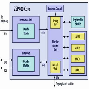
Author: Single Core Microprocessor architecture With the demand for high-performance computing, the computer architecture has undergone great changes. As a core component of a microprocessor, its performance and complexity (number of transistors, clock frequency, and peak value) also grow in accordance with Moore's Law. The improvement in microprocessor performance is due in large part to the development of architectures and improvements in VLSI technology. The development of the architecture is mainly reflected in three aspects: super-flowing water, multi-instruction transmission, and multi-instruction operations. Super-flowing water technology mainly develops time parallelism. Pipelining is an important feature of RISC processors that distinguish them from CISC processors. Using superfluid technology, although it can reduce the time of each stage in the critical path, it also introduces more registers, which increases the area overhead and clock skew issues. On the other hand, deep pipelines significantly reduce the performance of the pipeline when it comes to instruction dependencies and instruction jumps. Multi-instruction transmission and multi-instruction operations are all development space parallelism. The primary issue facing multi-instruction transmission is how to maintain the correctness of application semantics. MIMD, superscalar, and data flow technologies are typical architectures for multi-instruction transmission. MIMD is an important research area for parallel computing. Super-scalar use of sequential instruction stream transmission technology, good compatibility, hardware overhead, power consumption, is the mainstream technology used by most commercial high-end processors. The use of token ring technology for data flow can theoretically develop high instruction parallelism. However, its commercial development was unsuccessful due to the large runtime overhead, especially the high cost of the token ring matching. Multi-instruction operation is an important research direction of the current architecture. Multi-instruction operations include data parallelism development and operational parallelism development. Although these two technologies have been adopted in CISC processors, CISC has brought three negative impacts on the development of the architecture: First, the CISC instruction is not suitable for pipeline processing, and the second is that the instructions are very different and cause difficulty in decoding. The third is compilation. It is difficult for the device to develop effective instruction operations. Contrary to the CISC processor, multi-instruction operation is well suited for RISC processors, where SIMD and VLIW are typical structures for data parallelism and operational parallelism. Both vector processors and SIMD processors use multiple operands to achieve data parallelism. But the two are very different. The vector processor operates on linear vector elements sequentially, and SIMD performs concurrent operations on vector elements. For the former, each instruction can only be applied to one functional component and the execution time is longer; the latter can act on multiple functional components when executing the instruction. The vector processor uses cross-memory to implement vector fetch operations, and at the same time, it can perform effective operations on short vectors, that is, compress sparse vectors to obtain high performance. SIMD is suitable for packet data streams in multimedia, and the long data stream is cut into fixed length and short vector sequences by a specific algorithm, so that efficient processing of fixed length and short vector sequences can be implemented like a vector processor. VLIW is an important way to achieve operational parallelism development. The CISC processor employs vertical coding techniques, while VLIW employs horizontal coding techniques. Each operation field in the instruction can be executed concurrently. Compared with the CISC processor, VLIW has the advantages that the instruction operation domain is fixed and the decoding is simple; it is suitable for stream processing and reduces the CPI; the compiler needs to develop the potential instruction-level operation parallelism of the program. The disadvantage of the traditional VLIW is that the instruction bandwidth is high and the binary object code is not compatible. Both VLIW and SIMD structures can accept a single instruction stream, and each instruction can contain multiple operations. However, the former allows each instruction to contain multiple different types of operations, while fine-grained parallelism can be developed. The VLIW instruction word is longer, and SIMD has a very strong data compression capability. In fact, the combination of VLIW and SIMD technology can achieve higher performance speedups and is very suitable for multimedia data processing. From the perspective of microprocessor architecture and compiler interface, instruction-level architecture can be divided into three categories: sequential structure, related structure, and independent structure. In the sequential structure, the program does not contain any instruction parallel information, and is completely scheduled by hardware. That is, the hardware is responsible for the correlation analysis, independent operation analysis and operation scheduling among the operations. The compiler is only responsible for the reorganization of the program code, and no information is attached to the program. . Superscalar is a typical representation of this type of structure. In the related structure, the program explicitly specifies the relevant information for the operation, that is, the compiler is responsible for the correlation analysis between the operations, while the hardware is responsible for the independent operation analysis and scheduling, such as the data flow processor. The independent structure is entirely provided by the program to provide information between independent operations, that is, the compiler is responsible for inter-operation correlation analysis, independent operation analysis and instruction scheduling. VLIW is its main representative. Superscalar processor architecture Modern superscalar processor architectures are based on the Dynamic Scoreboard technology used by Tomasulo and CDC6600 used in IBM 360/91. The MIPS R10000 and DEC21264 microprocessors are based on this architecture. Typical superscalar processors typically use the following logical structure for dynamic scheduling: register renaming logic, window wakeup logic, window selection logic, and data bypass logic. Intel's Pentium processor, Motorola's PowerPC 604 and SPARC64 use a superscalar architecture based on reserved stations. The main difference between the two architectures is that in a typical superscalar architecture, both speculative and non-speculative register values ​​are placed in the physical register file; in the superscalar structure of the reservation station, the speculative data is placed in the reorder buffer. Non-speculative data and data that has already completed the commit are placed in the register file. In a typical structure, the operands are not broadcast to the window, but only the operand flag TAG is broadcast, and the operand is sent to the physical register file. In the reservation station structure, the instruction execution result is broadcasted to the reservation station, and the instruction is transmitted from the reservation station to fetch the operand. Superscalar processor performance is proportional to the product of IPC (Instructions Per Cycle) and clock frequency. The clock rate is related to the critical path delay of the system structure, and the IPC is related to the following factors: potential instruction-level parallelism, architecture word length width, instruction window size, and parallelism development strategy in the program. Superscalar processors generally increase IPC by adding transmit logic, which will lead to wider transmit windows and more complex transmit strategies. As we all know, the superscalar processor is the mainstream architecture of general-purpose microprocessors. Almost all commercially available general-purpose microprocessors use a superscalar architecture. On the DSP side, LSI Logic's ZSP200, ZSP400, ZSP500, and ZSP600 all use a superscalar architecture. ZSP200 adopts parallel MAC and ALU operation components, 2 transmit superscalar structure; ZSP400 adopts dual MAC unit, 4 transmit superscalar processor architecture; ZSP500 has 4 transmit architecture, adopts enhanced dual MAC and dual ALU operation unit; ZSP600 adopts The 4MAC and dual ALU operation components emit 6 instructions per clock cycle. Figure 1 shows the block diagram of the ZSP400. ADI's TigerSHARC series uses a static superscalar architecture. The series uses many of the features of traditional superscalar processors, such as load/store structures, predictions, and interlocked register files. Four instructions are fired per clock cycle. The meaning of static superscalar is that instruction-level parallelism is identified before running, that is, when writing a program (in fact, based on the VLIW structure). At the same time, Tiger SHARC system processors use SIMD technology, users can broadcast and merge data. All registers are interlocked and support a simple programming model that does not depend on the delay variation between different models. The branch target buffer BTB is 128 bits, which can effectively reduce the cycle time and other non-sequential code execution time. Figure 2 shows the block diagram of the ADSP-TS201S in the TigerSHARC series. Very Long Instruction Word VLIW Architecture Since JA Fisher of Yale University first proposed the VLIW architecture in 1979, Yale University has developed the MultiFlow processor based on Trace Scheduling and the block-based scheduling developed by Bob Rau et al. (Cydrome). ) The Cydra-5 processor. However, until the mid-1990s, processors based on VLIW architecture basically remained in the laboratory prototype stage. Because several key issues inherent in the VLIW itself have not been completely resolved, resulting in the subsequent commercial processor architecture from RISC to superscalar and superfluid water, rather than VLIW. However, due to the many advantages of the VLIW architecture, many research institutes still competed for the technology and made breakthroughs in the architecture and compiler. Among them, the most important is to solve the target code compatibility problem and support inference. Speculation mechanism (although most processors only support partial inference speculation mechanisms). This followed Philip's Trimedia, Equator's MAP1000A Media Processor, Chromatic's Mact, TI's TMS320C6XX, Transmet's Crusoe, and the Intel and HP Alliance's proposed IA-64 architecture (EPIC). In fact, VLIW has become a consensus as the preferred technology for the next generation of high-performance processor architectures. The SIMD instruction flow formed by the architecture and optimized compiler will be more suitable for multimedia data processing. TI's TMS320C6 family is a typical ultra-long instruction word VLIW architecture that can execute eight 32-bit instructions per instruction cycle, C62 is a fixed-point processor, and C67 is a floating-point processor. The CPU cores of the C62 and C67 series are the same and contain 32 general-purpose registers and 8 execution units. C64 contains 64 general purpose registers and 8 execution units. The 8 execution units contain 2 multipliers and 6 ALUs. Supports 8/16/32 data types, all instructions are conditional execution, reducing branch instruction overhead. Figure 3 shows a block diagram of the C62 and C67 systems. The Institute of Acoustics, Chinese Academy of Sciences, has successfully developed the first domestic high-performance microprocessor-based SuperV processor based on multi-emission VLIW and SIMD technology, funded by the “973 National Major Basic Research Development Planâ€. The processor is a four-shot VLIW processor that performs 35 operations per cycle when performing vector processing functions. Obtained when performing 32-bit multiply-accumulate operation of the data processing speed of 2.9 GOPS; performing data processing speed of 5.1 GOPS obtained when 16-bit multiply-accumulate operation; performing data processing speed can be obtained when 9.3 GOPS 8 multiply-accumulate operation. The processor is currently the most powerful microprocessor in domestic data processing capacity and can be widely used in signal processing fields such as information appliances, network communications, sound images, and radar sonar. Reconfigurable processor architecture Since the first generation of CISC processors began in the 1970s, the microprocessor architecture has gone through three generations. However, even the third-generation RISC technology still remains in the fixed-mode architecture design. With the development of ASIC and SOC technologies, microprocessor design has entered the fourth generation, namely the post-RISC and reconfigurable processor era. Its important feature is that the system architecture no longer uses a fixed mode, but combines the flexibility of the DSP with the specificity of a hardwired connection, so that the microprocessor can build its own unique architecture for different application requirements to achieve optimal performance. The purpose of lower power consumption. SuperV architecture is not only based on RISC, VLIW, and SIMD technologies, but also adopts reconfigurable technology, which enables users to complete processing of different applications through the reconstruction of system functional components without increasing hardware overhead. Not only improves the system performance, but also greatly reduces the power consumption of the system. For example, a number of 32-bit reconfigurable multipliers are designed in Warwick processors, each of which can perform 32-bit multiplication, several 16-bit multiplication, or 8-bit multiplication. Therefore, the Warwick processor can use a single instruction to complete the multiply and accumulate operation of 16 8-bit data; one instruction can complete the multiply and accumulate operation of 8 16-bit data; one instruction can complete 4 32-bit data. Multiply and add operations; one instruction can complete the accumulation of four 32-bit data; one instruction can complete 16 indexes, 16 address calculations, and 16 data load operations; two instructions complete 16 8-bit data accumulation operations; The instruction can complete eight 16-bit data accumulating operations; two instructions can complete the 16-way parallel search of 256- and 8-bit element data tables. Tensilica's configurable technology is an important representation of reconfigurable processors. For example, the Vectra LX fixed-point vector DSP engine is built on configuration options based on the Xtensa LX configurable processor. That is, the Vectra LX fixed-point DSP engine is a configuration of the Xtensa LX microprocessor core. The fixed-point DSP engine is a 3-transmit SIMD processor with four multiplier/accumulators (four MACs), which can handle 128-bit vectors. A 128-bit vector can be divided into 8 16-bit or 4 32-bit elements. Whole Vectra LX DSP engine with TIE (Tensilica's Instruction Extension) language developed by modifying suitable for different applications. The Vectra LX DSP Engine adds 16 vector registers (160 bits wide per register), four 128-bit vector queue registers, a second load/store unit, and more than 210 existing Xtensa LX processor instruction set architectures General DSP instructions. The Vectra LX DSP engine is shown in Figure 4. Concluding remarks As the core technology of the information industry, the microprocessor architecture is undergoing great changes, and this change all reflects the strong driving force of market demand. Modern microprocessors, whether general microprocessors or digital signal processors, are tending to converge in architecture. General-purpose processors increase the capabilities of data processors by adding media processing instructions; digital signal processors also draw on the architecture of general-purpose processors, making the digital signal processor's data processor more powerful and more manageable. At the same time, with the needs of embedded applications, the requirements for power consumption are becoming more and more demanding, making reconfigurable processors an important role in the future. Due to different application requirements, the required microprocessor system architecture can be obtained through the reconstruction technology, which will greatly increase the competitiveness of the product and at the same time reduce the power consumption and cost of the entire system. Perkins 401-999KW Diesel Generator Perkins 401-999KW Diesel Generator,Perkins Shanghai genset,Perkins Shanghai Power Generator,Perkins Power Generator Set Shanghai Kosta Electric Co., Ltd. , https://www.generatorkosta.com
Figure 1 ZSP400 core superscalar architecture block diagram 
Figure 2 ADSP-TS201S static superscalar architecture block diagram 
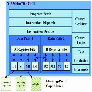
Fig. 3 System block diagram of TMS320C6 based on VLIW architecture 
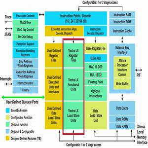
Figure 4 Vectra LX DSP architecture block diagram
Looking at the Development Trend of High Performance Microprocessors from the Evolution of Architecture
Looking at the Development Trend of High Performance Microprocessors from the Evolution of Architecture