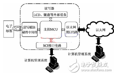
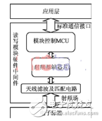
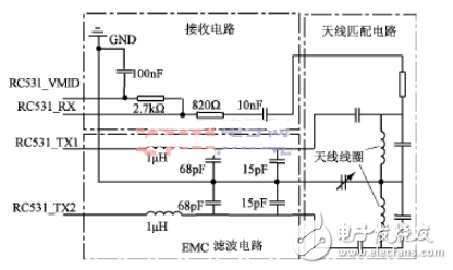
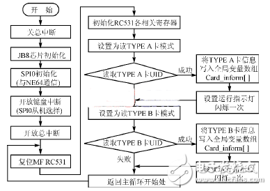
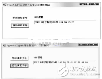
Radio frequency identification is a non-contact automatic identification technology, which has been widely used in logistics, manufacturing, public information services and other industries; and the networking of embedded systems has become an important feature of the PC era. Therefore, the combination of RFID technology and embedded Ethernet technology has become one of the hot topics in academic research. According to the status of domestic RFID applications and market demand, this design reads the globally unique serial number UID of the radio frequency chip in the second-generation ID card, and uses the second-generation ID card instead of the traditional read-only electronic tag, which saves the cost of the card. The structure of the reader with Ethernet communication function is shown in Figure 1. Figure 1 Reader structure with Ethernet communication capabilities The RFID system consists of a reader and a computer management system. Among them, the reader has a core role and is also the focus of this research. It obtains the UID information of the second-generation ID card through radio frequency, and transmits it to the computer management system via Ethernet to ensure the stability and security of the entire RFID system. The role of the decision; computer management system to receive the UID information sent by the reader, for different applications to make the appropriate processing and control. According to system functional requirements, the reader hardware system is divided into two parts: the read-write module hardware middleware and the master control system with Ethernet communication function. This design can not only facilitate the debugging of the two parts independently, but also can reduce the signal interference between the two parts and improve the reusability of the hardware module. 2.1, reading and writing module hardware middleware Referring to the common definition of middleware, combined with the characteristics of embedded systems, the hardware structure of the read-write module hardware is designed, as shown in FIG. 2 . The differences in hardware environments such as electronic tags and radio base station chips are shielded downwards, and standard software and hardware interfaces are provided for the RFID application layer. The development of the application layer is based on this interface. It does not need to consider the implementation details of RFID, and regardless of how the underlying hardware is upgraded, only the middleware needs to be upgraded and updated, and the external interface definition of the middleware remains unchanged. The application software is almost unnecessary. Make any changes to provide a relatively stable high-level application environment. Figure 2 read-write module hardware middleware structure (1) Connection between a microcontroller and a radio base station chip The system uses MFRC531 as a radio base station chip. The chip is a member of the highly integrated IC read/write chip series for 13.56 MHz non-contact communication produced by NXP. Freescale's low-cost, high-performance MC68HC908JB8 (abbreviated as JB8) is used as a modular microcontroller. It connects to the RF base station chip MFRC531 through SPI communication and controls the completion of reading electronic label UID information. The MFRC531 supports SPI communication and acts as a slave during communication. There is no integrated SPI module inside the control chip JB8, and its communication function is simulated by the I/O port software. (2) Antenna design In an RFID system, a radio base station chip (such as MFRC531) transmits energy through an antenna and performs data communication with an electronic tag. The design of the antenna is very important to the stability of the communication. This design uses the direct matching antenna method. The circuit design is shown in Figure 3. Figure 3 RF antenna circuit principle 2.2, main control system hardware design The main control system and the read-write module are connected through the SPI interface to obtain the electronic tag information stored in the module control chip memory, and then the information is transmitted to the computer management system through the Ethernet communication interface. The system adopts Freescale's 16-bit MCUMC9S12NE64 as the main control chip. The internal integrated EMAC (Ethernet Media Access Controller, Ethernet Media Access Controller) and EPHY (Ethernet Physical Transceiver, Ethernet physical layer transceiver) can be implemented with the third-party TCP/IP protocol stack to realize the ether The communication function of the network enables a single-chip Ethernet connection scheme. The software design of the system mainly includes the software design of the read-write module and the software design of the embedded Ethernet. The reading and writing module mainly realizes the UID identification of the TYPEA&B electronic tag; the embedded Ethernet part realizes the communication of the Ethernet. 3.1, read and write module software design The read-write module is designed as a hardware middleware that provides an interface for data interaction between the application system and the electronic tag. The main function flow of the module microcontroller MC68HC908JB8 is shown in Fig. 4. After the system is powered on, it first executes the initialization of the MCU and related modules, and then enters the main loop. As shown in FIG. 4 , the card reading mode is continuously switched in the main loop to meet the requirement of reading the UIDs of the two types of electronic tags TYPEA&B. Once successful, the UID is assigned to the global byte array variable Card_inform[]. Card_inform[0] stores the type of the electronic tag, ie the ASCII code of "A" or "B", followed by the UID of this type in turn. The main control system can obtain the contents of Card_inform[] through the SPI communication interface of the read/write module hardware middleware. After the acquisition is completed, JB8 clears the Card_inform[] array. The reset and register initialization operations of the RC531 were originally placed before the main loop, that is, only once after the JB8 reset. However, in the actual testing process, when the RC531 is running for a long time, instability will occur. Therefore, these two operations are placed in the main loop to improve the robustness of the system. Figure 4 read and write module main function process 3.2, embedded Ethernet module software design The integrated EMAC and EPHY modules within the MC9S12NE64 can implement data link layer functions. In order to realize the communication of Ethernet, have designed a streamlined embedded TCP/IP agreement that does not need the operating system, has realized the Ethernet access function of MC9S12NE64. When migrating the protocol stack, as long as the driver implementation part is modified and the call interface remains unchanged, the upper layer protocol can be unchanged. The entire protocol stack operates in a circular manner. The MC9S12NE64 receives Ethernet frames in an interrupt mode. The protocol stack filters the received Ethernet frames from the bottom up and processes them accordingly. The layers are designed as follows: 1 link layer - MC9S12NE64 Ethernet driver, ARP protocol; 2 Network layer - IP protocol, ICMP echo reply service; 3 Transport layer - UDP protocol. 3.3, UID identification test of TYPEA&B electronic tags Figure 5 shows the test results for identifying the UIDs of the two TYPEA&B tags. Figure 5 UID identification test results for TYPEA&B electronic tags The PC actively sends UDP datagrams containing communication commands to the reader. After receiving the datagram, the reader/writer returns the latest UID information obtained to the PC host through the UDP protocol. The specific parameters of the test are listed in Table 1. Table 1 UID identification test parameters
WARNING!
Do not plug two or more meters together!
IMPORTANT
Don't plug in an appliance where the load
exceeds 16 Amp. Always ensure the plug of any appliance is fully
inserted into the meter outlet. If cleaning of the meter is required,
remove from mains power and wipe meter with a dry cloth.
KEYBOARD DEFINITION
1). SET: Set price with button UP.
2). MODE: Exchange display state.
3). UP: Set price combined with button SET.
GENERAL FEATURES
1).Display line power.
2).Display and memory accumulative total power quantity.
3).Display and memory total power charge of price.
THE DATA DISPLAY
Press MODE button the data displays as follows:
W →KWh →PRICE →COST/KWH
↑_ _ _ _ _ _ _ _ _ _ _ _ _ _ _ _↓
1). Plug in socket and power on, the meter will display real power.
2). Press MODE button once again and release, the meter will display accumulative KWh.
3). Press MODE button once again and release, the meter will display total power charge.
4). Press MODE button once again and release, the meter will display COST/KWH.
SETTING PRICE OF COST/KWH
1). Press SET button during display COST/KWH,the first digital COST/KWH flash, press UP button to set it.
2). Press SET button once again and release, the second digital COST/KWH flash, press UP button to set it.
3). Press SET button once again and release, the third COST/KWH flash, press UP button to set it.
4). Press SET button once again and release, the fourth COST/KWH flash, press UP button to set it.
5). Press SET button once again and release, the radix point COST/KWH flash, press UP button to set it.
DATA CLEAR
Press and hold MODE button for 5 seconds will clear KWH,PRICE and COST/KWH data.
Power Meter Plug Energy Monitor,Backlight Power Metering Socket,Blue Backlight Power Meter Socket,Multi-functional Backlight Power Meter Socket NINGBO COWELL ELECTRONICS & TECHNOLOGY CO., LTD , https://www.cowellsockets.com