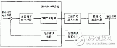
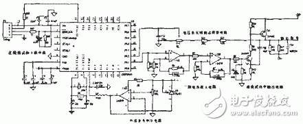
When testing a type of launcher. Three sets of accurate DC voltage signals based on 11.50 volts are required. In order to cooperate with the test process, these three sets of signals need to take 18 different DC voltage values ​​in different time periods, and the amplitude distribution is within the range of 9.33 to 1.13 volts. The original tester uses a voltage divider of 22 precision resistors to match the band switch selection to produce these 18 different precision DC voltage signals. This design method is expensive and cannot be automated, and the test steps need to be switched by manually dialing the band switch. In order to achieve automatic testing of the launch device. A new type of detector was designed using microcomputer technology. The new inspector takes the CPU module as the core and generates these three sets of accurate DC voltage signals through program control D/A converters, which simplifies the design, reduces the cost, and realizes the automatic switching of the test steps. However, during the use of the detector, it is found that the RTEX phenomenon often occurs, that is, the detector determines that a certain piece of equipment is unqualified, but the result is good when the instrument is replaced or restarted. This situation seriously affects the use and maintenance of the equipment unit. After analysis. It is considered that the analog circuit which mainly produces these three sets of accurate signals in the detector has a problem of operating point drift, and the precision is not high. The voltage output is unstable, resulting in an incorrect test status. In order to solve this problem, this paper is based on C8051F410 microcontroller. A new precise signal analog circuit is designed by PWM modulation technology and negative feedback measurement technology, which effectively suppresses the drift of the working point and improves the output precision of the analog circuit. Solved the practical problems in the maintenance and use of equipment. The circuit design uses a closed-loop control structure, as shown in Figure 1. The circuit is based on C8051F410 microcontroller. The initial parameter of the output voltage is set by the program, and the programmable counter array (PCA) inside the single chip microcomputer is controlled to generate a PWM waveform with an appropriate duty ratio, and the second DC signal amplifying circuit and the push-pull output circuit are amplified to obtain an accurate DC voltage signal. . In order to suppress the drift of the dead point and ensure sufficient output precision, the output signal is divided and then led back to the C8051F410 microcontroller, and the voltage is measured by the internal digital-to-analog converter of the microcontroller, and compared with the initial setting parameters. Adjust the duty cycle of the PWM waveform through the program. Thereby, a DC voltage output signal with high reliability and high precision is obtained. The basic idea of ​​this circuit is to use the PWM port of the single-chip microcomputer, without changing the PWM square cycle. The PWM control register of the microcontroller is adjusted by a software method to adjust the duty cycle of the PWM to obtain the required voltage signal. The MCU required by this circuit must have two necessary conditions, ADC port and PWM port. The number of bits of the ADC is as high as possible, and the working speed of the MCU is as fast as possible. Before adjusting the output voltage, the MCU first reads the output voltage quickly. Then, the set output voltage is compared with the actually read output voltage. If the actual voltage value is too small, the PWM duty ratio is adjusted in the direction of increasing the output voltage: if the actual voltage is too large, the output is reduced. The direction of the voltage adjusts the duty cycle of the PWM. After selection, the C8051F410 microcontroller processor has a maximum operating clock of up to 50MHz: it has 6 PCM modules. It can realize PWM output; it has a 12-bit ADC module to meet the requirements of voltage measurement accuracy. The hardware design of the whole circuit mainly includes three parts of peripheral circuit design, amplifier circuit design and voltage feedback measurement pre-circuit design of C8051F410 single chip microcomputer. as shown in picture 2. The entire circuit is based on the C805IF410 microcontroller. The C805IF410 microcontroller features P0, P1, and P2 digital/analog configurable I/O ports. All digital and analog resources can be used with these three sets of 24 I/O pins. To output an accurate analog signal, you need to set one pin as the PWM output port and one as the ADC input port. Here, we set PO.1 as the PWM output port and P0.2 as the ADC input population. The peripheral circuit design of C8051F410 MCU mainly includes online debugging and downloading circuit, external reference voltage circuit and filter circuit design. This paper designs the online debugging and downloading circuit by using the C2 debugging interface provided by the single chip microcomputer. As shown in the upper left circuit of Figure 2. The fast programming of the MCU and the online debugging of the system are realized through the serial port of the computer. On the right side of Figure 2, the external reference voltage circuit is connected to the Vref pin of the microcontroller. Provides a 2.048 volt reference for modules such as microcontrollers. It can be adjusted by a potentiometer. The amplifying circuit comprises two parts of a secondary voltage amplifying circuit and a push-pull power output circuit. As shown in the circuit on the right side of Figure 2. The secondary signal amplifying circuit and the push-pull output circuit are classic circuits, and are not described herein again. The voltage feedback measurement pre-circuit is shown in the upper part of the right side of Figure 2, which is essentially a voltage divider circuit. Since the reference voltage of the C8051F410 MCU is set to 2.048 volts, and the maximum output voltage is about 12 volts, the resistor R15=4.3K, R16=20K, the nominal resistance of the potentiometer Pv1 is 5K, and the potentiometer can be adjusted. To change the voltage multiple. Ceramic Housing Ceramic Housing YANGZHOU POSITIONING TECH CO., LTD. , https://www.cndingweitech.com
