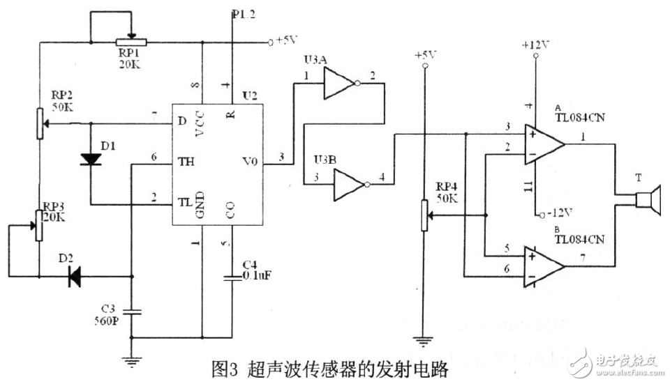
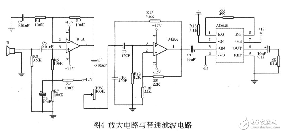
Ultrasonic waves are mechanical waves with a frequency above 20 kHz and a propagation velocity in air of approximately 340 m/s (at 20 °C). Ultrasonic waves can be generated by ultrasonic sensors. Two types of ultrasonic sensors are commonly used: one is to generate ultrasonic waves electrically, and the other is to generate ultrasonic waves by mechanical means. Currently, piezoelectric ultrasonic sensors are commonly used. Because ultrasonic wave has easy directional emission, good directionality, good intensity control, insensitivity to color and illuminance, and high reflectivity, it is widely used in non-destructive testing, distance measurement, distance switch, car reversing collision, intelligent robot and other fields. . The overall block diagram of this design is shown in the figure, mainly consisting of ultrasonic transmission, ultrasonic reception and signal conversion, key display circuit and temperature sensor circuit. The ultrasonic ranging is to continuously detect the echo reflected by the obstacle after the ultrasonic wave is emitted, thereby measuring the time difference T between the transmitting and receiving echoes, and then finding the distance S=CT/2, where C is the ultrasonic wave velocity. At normal temperature, the speed of sound in the air is about 340 m/s. Since the ultrasonic wave is also a kind of sound wave, its propagation speed C is related to the temperature. When it is used, if the temperature does not change much, the sound speed can be considered to be substantially constant. Because the accuracy of the distance measurement of this system is very high, the propagation speed of the ultrasonic wave is corrected by detecting the temperature. After the ultrasonic wave propagation speed is determined, the distance can be obtained by measuring the time of the ultrasonic wave back and forth. This is the basic principle of the ultrasonic ranging system. Ultrasonic signal transmitting and receiving circuit The transmitting part circuit is shown in FIG. 3, and is mainly composed of a pulse modulation signal generating circuit, an isolating circuit and a driving circuit for providing a transmitting signal for the ultrasonic sensor. In the pulse modulation signal generating circuit, the reset (RESET) terminal of the 555 is controlled by the single chip microcomputer, so that the 555 timer works in time to generate a pulse modulation signal with a pulse frequency of 40 KHz and a period of 30 ms, and the signal waveform is as shown in FIG. 2 . In this design, 10 pulse signals are transmitted in one cycle. The isolation circuit is mainly composed of two NAND gates to isolate the output stage from the pulse generation circuit. The output stage consists of two general-purpose integrated operational amplifiers, the TL084CN. Since the ultrasonic sensor's emission distance is proportional to the voltage applied across it, the circuit is required to generate a sufficiently large driving voltage. The basic principle is a comparison circuit when input. When the signal is greater than 2.5V, the output voltage of the op amp A is VA=+12V, the output voltage of the op amp B is VB=-12V, and when the input signal is 2.5V, the output voltage of the op amp A is VA=“-12Vâ€. The output voltage of the operational amplifier B is VB=+12V, so two symmetric waveforms with opposite polarities are obtained at both ends of the ultrasonic sensor, that is, VB=-VA, so the voltage applied across the ultrasonic sensor is V=VA-VB=2VA. The voltage across it can reach 24V, which ensures that the ultrasonic wave can transmit a long distance and increase the measurement range. The circuit of the receiving part is composed of an amplifying circuit, a band pass filtering circuit and a signal conversion circuit. The amplifier circuit and band pass filter circuit are shown in Figure 4. Since the ultrasonic signal is greatly attenuated when it propagates in the air, the reflected ultrasonic signal is very weak and cannot be directly sent to the subsequent circuit for processing. The signal must be amplified to a sufficient amplitude to make the subsequent circuit pair It does the right thing. The preamplifier circuit is a bootstrap type non-inverting AC amplifier circuit composed of an integrated operational amplifier. It has a high input impedance. C5, C6, and C7 are DC blocking capacitors. R5, R6, and R7 are bias resistors. Static working point. The bandpass filter uses a second-order RC active filter to eliminate the effects of interfering signals received during ultrasonic propagation. Amplifying circuit and band pass filter circuit The circuit is a second-order voltage-controlled voltage source band-pass filter circuit. In the figure, RW and C10 form a low-pass filter network, and C9 and R12 form a high-pass filter network. The two are connected in series to form a band-pass filter circuit. The integrated op amp and resistor R9, RlO together form the same amplifier. In order to make the circuit work stably, the gain of the same amplifier must be guaranteed. The center frequency of the bandpass filter is ω0=40kHz, and the circuit parameters can pass AV=1+R9/ R10 and ω0=1/R12C2 (1/RW+1/R13) are determined. The signal after bandpass filtering is amplified by the dedicated instrumentation amplifier AD620, and then sent to the signal conversion circuit. The signal conversion circuit mainly converts the received envelope signal into an interrupt trigger signal of the single chip microcomputer. It consists of an envelope detector circuit, a voltage comparator and an RS flip-flop. The envelope detection circuit consists of a diode D3, a resistor R19, and a capacitor C13. The signal obtained by envelope detection is shown as V2 in Fig. 6. The voltage comparator consists of an integrated op amp and a capacitor resistor. To eliminate the interfering signal from the transmitter, we add the signal from the microcontroller P1.2 to the non-inverting terminal of the voltage comparator. The waveform is 250μs high and 29750μs. A low-level square wave isolates P1.2 from the forward side of the comparator through diode D3. When P1.2 outputs a high level, the capacitor C14 is charged through the diode. Since the diode is forward-conducting, the charging is fast. When the P1.2 output is low, the diode is reversed and the capacitor is discharged through the resistors RW and R21. Because the total resistance is relatively large, the discharge is very slow. The waveform is shown as V3 in Figure 6. As can be seen from the figure, when the return signal is not received, the comparator outputs a high level. If a return signal is received, the comparison is made. The device outputs a low level, and the output waveform is as shown by Vo in Fig. 6. In this way, the interference of the transmitting probe on the reflected signal can be eliminated. Global Electronic Measurement Technology and Market Leader - Keysight (formerly Agilent Electronic Measurement Division) Micro USB 3.0 Male,Micro USB 3.0 Straddle Type,B Male Straddle Type 0.8mm,MICRO USB 3.0 B MALE ShenZhen Antenk Electronics Co,Ltd , https://www.antenksocket.com

We are manufacturer of Micro USB 3.0 Male in China, if you want to buy Micro USB 3.0 Straddle Type,B Male Straddle Type 0.8mm,MICRO USB 3.0 B MALE please contact us.
USB3.0 is a USB specification, which was initiated by Intel and other companies. The maximum transmission bandwidth of USB3.0 is as high as 5.0gbps (500MB / s).
While maintaining compatibility with USB2.0, USB3.0 also provides enhancements: significantly increased bandwidth (up to 5Gbps full duplex); better power management;
more power; faster device identification; and higher data processing efficiency.
The reason why USB 3.0 has the performance of "speeding" is entirely due to the improvement of technology.
Compared with USB 2.0 interface, USB 3.0 adds more physical buses in parallel mode.
You can pick up a USB Cable and look at the interface.
On the basis of the original 4-wire structure (power supply, ground wire, 2 pieces of data), USB 3.0 adds 4 lines for receiving and transmitting signals.
So there are eight lines in the cable and on the interface.
It is the additional 4 (2 pairs) of lines that provide the bandwidth required for "superspeed USB" to achieve "over speed".
Obviously, two (1 pair) lines on USB 2.0 are not enough.
In addition, in the signal transmission method, the host control mode is still used, but the asynchronous transmission is changed.

USB 3.0 makes use of two-way data transmission mode instead of half duplex mode in USB 2.0 era. In short, data only needs to flow in one direction, which simplifies the time consumption caused by waiting.

In fact, USB 3.0 does not take any rarely heard of advanced technology, but theoretically increases the bandwidth by 10 times. As a result, it is more friendly and friendly. Once superspeed USB products come out, more people can easily accept and make better customized products.