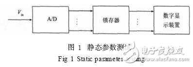
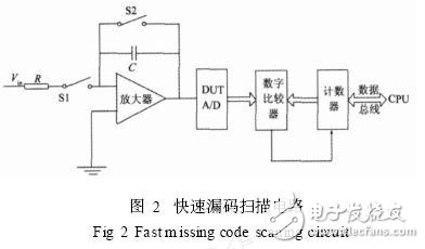
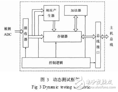
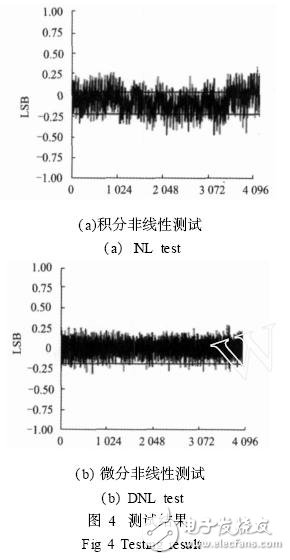
With the continuous development of digital technology and the widespread use of computers in the fields of signal processing, control, etc., the work done by analog circuits in the past is increasingly being processed by digital circuits or computers today. As a bridge between analog and digital, the importance of analog-to-digital converters (ADCs) has become increasingly prominent, which has also driven the development of ADC test technology. This paper first introduces the ADC test, including static parameters and dynamic parameter test, and then combines the automatic test system test examples to detail the test process of the ADC chip parameters. 1. 1 Test principle of static parameters The static parameters of the ADC refer to various performance parameters measured at low speed or DC flowing into the ADC chip. The static parameter test method has a point-by-point test method, etc., and the main test process is shown in FIG. (1) Measurement of zero error The zero point error, also known as the input offset, is the maximum error of the code midpoint of the number 0 in the actual analog-to-digital conversion curve and the midpoint of the code of the number 0 in the ideal analog-to-digital conversion curve, denoted as EZ. The test method is as follows: the input voltage is gradually increased. When the digital display device in FIG. 1 is changed from 00..00 to 00..01, the input voltage Vin1 is recorded at this time, and then the input voltage is gradually decreased to make the digital display device Change from 00..01 to 00..00, write down the input voltage Vin2: Where: N is the number of A / D bits; VFSR is the full-scale value of the A / D input voltage, LSB is the least significant bit of the ADC. (2) Gain error EG measurement The gain error is the deviation between the actual slope of the conversion characteristic curve and the ideal slope. The test method is as follows: adjust the zero error to 0, and the input voltage changes from full scale, so that the digital output changes from 11..11 to 11..10, which is recorded as Vin1. The Vin is gradually changed in the opposite direction, so that the output is changed from 11..10 to 11..11, and the input voltage Vin2 is recorded. then: (3) Measurement of linearity error Linear error is the maximum deviation between the actual conversion curve and the ideal characteristic curve. The actual measurement is to test the code center value of the jth code, and compare it with the center value of the ideal j code. The test method is as follows: 1. Adjust the input voltage so that the digital output is changed from the jth code to the j-1th code. For Vin1; 2 adjust the input voltage, so that the digital output is changed from the j-1th code to the jth code, which is recorded as Vin2; 3 adjust the input voltage, so that the digital output is changed from the jth code to the j+1th code. For Vin3; 4 adjust the input voltage, make the digital output from the j + 1 code to the jth code, denoted as Vin4; 5 find the deviation of the jth code ΔVj is: Where: Vj is the nominal quantized value of the jth code of the ADC in the ideal state; 6 repeating the above steps, the deviation of all the numbers is measured, and the maximum value of the absolute value Δ_Vj− is the linear error. (4) Measurement of differential linearity error The differential linearity error is the maximum deviation between the code width of the actual conversion characteristic curve and the ideal code width. In fact, the measurement of linear error and the measurement of differential linearity error are performed simultaneously. Find the measured value of the analog voltage corresponding to the measured point N, and then find the measured value of the analog voltage corresponding to N + 1, the difference between the two. This is the code width of the actual conversion curve at that point. From the jth digital value to the digital value of the j+1 code, the difference between the actual analog Vin1 input value, the difference between the difference and the ideal step size of 1 LSB, and then the maximum value is the differential linearity error. . That is, the actual code width Δj of the jth code is measured: Comparing Δj with 1 LSB, the absolute value of the deviation is the differential linear error to be measured. 1. 2 Principles of testing dynamic parameters The dynamic performance of the ADC includes many factors such as signal-to-noise ratio (SNR), signal to noise distortion ratio (SINAD), total harmonic distortion (THD), spurious-free dynamic range (SFDR), and dual tone intermodulation distortion (TTIMD). Wait. The test methods of dynamic parameters include dynamic signal superposition test method, spectral analysis FFT method and histogram method. (1) Dynamic signal superposition test method [ 526 ] Its basic idea is to superimpose a small AC signal on the reference voltage of the analog input of the A/D converter under test, so that the digital output of the A/D converter changes back and forth around the specified code at a certain frequency for a short time, thus testing Corresponding transition points and code center values ​​are derived, and zero point error, gain error, relative accuracy, and differential linearity error can be determined. This method is simple and easy, but it is limited by resolution and speed. (2) Spectral analysis FFT method A full-scale sinusoidal signal is sent to the ADC under test, and the converted result is stored in a memory, and then an FFT operation is performed on the output data to calculate parameters such as SNR and THD. The input consists of two sine waves of different frequencies, and the IMD can be calculated after performing the FFT operation. When testing high-precision ADCs, the length of the FFT is required to be sufficient, and the choice of test frequency is a key issue in the application of the FFT method. In addition, the FFT method requires that the sampling frequency cannot be an integer multiple of the signal frequency. The FFT method is a very common method in ADC dynamic testing. Its advantage is that it is intuitive and simple. The distortion of almost all ADCs can be expressed in its output spectrum. However, this method cannot avoid the impact of spectrum leakage and error sources other than ADC on the test. (3) Code density histogram method This method is to send a sine wave to the A/D converter under test, and the number of sampling points of the A/D converter is recorded by the computer, and then the computer performs calculation and processing through software to draw a histogram, thereby quantitatively Parameters such as differential linearity error, missing code, and gain error are shown. The following describes how to implement the ADC test on the BC3192V50 test system. The system is a VXI bus type digital-analog hybrid integrated circuit test system developed by Beijing Institute of Automatic Test Technology. The system has a maximum test rate of 50 MHz and provides 16-bit resolution and 100 KHz conversion/sampling rate, which can be triggered by digital system. The waveform generator, waveform analyzer and high-speed DSP processor have strong analog signal test and mixed signal test. 2. 1 test system hardware structure (1) Layer 1: Known as the “master machineâ€, it provides the most basic and common hardware resources needed to test various ICs. It includes: 1 power supply; 2 precision measurement unit (PMU) and programmable relay matrix; 3 precision voltmeter; 4 digital circuit part. (2) Layer 2: Adapter layer, which is a matching layer provided for the testing of certain types of devices on the basis of the large platform of the mother machine, and a dedicated test circuit for testing certain types of ICs. (3) Layer 3: The personality card layer is a small board designed to test a specific IC in a certain class. The adapter is a test circuit developed for a specific chip, and is the key to developing various chip tests. 2. 2 test system software Includes drivers for each instrument module, soft panel, debugger, user test program development environment, and test library. 3.1 single monotonic code scanning test 2. The test principle of static parameters has been mentioned in Section 1. It is easy to implement in this test system. The following is an example of a quick monotonic missing code scanning test to introduce the configuration of the test adapter. The fast missing code scanning circuit is shown in Figure 2. On the left side of the figure, the integration circuit is used to generate a monotonically rising or falling voltage. The rising or falling amplitude of the voltage is greater than the analog input voltage range of the DUT under test; the right side of the figure is composed of the digital quantity output by the DUT and the calculator. Digital comparison circuit. Before the computer scans the counter to the lowest value of the analog input voltage of the DUT through the data bus, the corresponding digital quantity is set to the number 0 here. At this time, the switch S1 is turned off, and S2 is closed, so that the analog input value of the DUT starts from 0. The input voltage to the integrating circuit is generated by the DAC, which is programmed to control the rate of voltage rise of the integrating circuit to match the conversion time of the device under test. The voltage rise rate is generally: when the output voltage of the integrating circuit increases, the time required for the output of the ADC of the device under test to be from the value D → D + 1 is approximately equal to 10 times the conversion time of the ADC of the device under test. When the scan starts, switch S1 is closed and S2 is opened, causing the integration circuit to be in a linear scan state. The device under test is periodically triggered to A/D convert the input signal. The output is compared to the counter. If they are equal, a pulse is generated by the digital comparison circuit to automatically "add 1" to the counter. During the scanning process, the computer continuously reads the counter value through the data bus and makes a judgment: if the counter should be "added 1" within the specified time, but not "added 1", the DUT is determined here. There is a missing code. The position of the missing code can be read only by reading the current value of the counter. If the counter is normally "added 1" within the specified time, and the count value of the counter reaches the maximum value of the DUT output of the device under test, the DUT has no leakage. code. 3. 2 Test the dynamic parameter code density histogram method and spectral analysis FFT method test environment configuration Based on the test host provides powerful DSP digital signal processing capabilities, this machine can also test dynamic parameters using code density histogram method and spectral analysis FFT method. The test principle is shown in Figure 3. The host high-precision signal source generates a sine wave or triangle wave and inputs the ADC to be tested. In the FFT test, after the ADC output digital is received by the receiver, the address generator sequentially generates the address and locks. The data latched by the memory is written to the memory, then transferred to the host, analyzed by the analysis software, and the test result is given. In histogram During the test, the data received by the receiver is taken as an address to retrieve data from the memory. The adder adds 1 and writes back to the same memory, and then completes the interface between the data and the host I/O bus. The control logic completes the control function of the entire operation. The test software completes the analysis of the data and gives the test results. The BC3192V50 test system is used to test the ADC. Figure 4 shows the test results of a 12-bit successive approximation ADC histogram. Figure 4 (a) shows the result of integral nonlinearity, and Figure 4 (b) shows the differential non- Linear result. The test results of the integral nonlinearity and the differential nonlinearity are controlled below 0.5 LSB. In this paper, based on the static and dynamic testing principle of ADC, the general process of ADC static parameters and dynamic parameters testing based on test system is given, and the process environment is analyzed in detail. Therefore, the low-cost, high-reliability computer-aided test of ADC is realized by the domestic automatic test system. Shenzhen Innovative Cloud Computer Co., Ltd , https://www.xcypc.com


