Video Display Signals and the MAX9406 DP-HDMI / DVI Level Shifter—Part II Abstract: This applicaTIon note is the second of a two-part arTIcle. Part II presents background on DVI ™ and display port (DP) interfaces. It then explains how the MAX9406 is used as a suitable digital-display cable driver with these interfaces. Part I (applicaTIon note 4306) examines the current TV and PC display-cable interfaces and covers the features of RGBHV, HDMI ™, and VGA. Both TV and PC displays are evolving toward a flat screen with digital-cable interface. A flat-screen TV can be connected to a PC or a high-definition TV (HDTV) set-top box using a high-definition multimedia interface (HDMI ) cable. A PC can be connected to an external monitor by a VGA or digital video interface (DVI) cable. The DVI can be considered the digital equivalent of a VGA interface. Note that the video portion of HDMI is identical to DVI. The DVI format can be considered as a digital version of VGA. Using a single or dual link, it supports higher resolution variations of VGA. Figure 1 shows the functional block diagram of a DVI plug-in card. Instead of the red, green, and blue DACs of the VGA plug-in card, here TMDS encoders, serializers, and LVDS drivers are used to produce high-rate bit streams and send the signals through three differential channels. Another LVDS differential channel is used for sending the clock signal of these bit streams. The DP is a more generalized and more capable interface than DVI. The DP can have one, two, or four high-speed differential pairs at a fixed bit rate of either 1.62Gbps or 2.7Gbps for a maximum speed of 10.8Gbps. The achieved video rate should be equal to, or lower than, the capabilities of all the differential pairs. Unused time slots are filled with extra / filling bits. The differential signal on each pair does not need to be LVDS compliant. The differential voltage can be 0.2 V, 0.4V, 0.8V, or 1.2V. The DC-bias voltage on each pin of the pair can vary from 0V to the power-supply level of the differential device driver. The differential signal is AC coupled, and the value of the AC-coupling capacitor can be from 0.075µF to 0.2µF. This capacitor provides flexibility for the IC implementation of the differential signal driver. The MAX9406 is a fast, low-skew, quad link, differential-input-to-differential-output signal level translator (Figure 6). It is designed for high-speed signal conversion of DP signals to DVI or HDMI signals. Each link of the device supports data rates up to 2Gbps. At the input ports, internal 50Ω termination resistors are available; a self-biased common mode matches the AC coupling of a typical DP differential pair. The MAX9406 also provides the voltage-level shift needed for HDMI's DDC and HPD pins; the level shift converts a 5V single-ended logic to 3.3V single-ended logic and vice versa. The MAX9406 offers an ESD rating of ± 2kV. The power-supply range is specified for 3.0V to 3.6V and operation is over the -40 ° C to + 85 ° C extended temperature range. The evolution of the analog VGA to the digital DVI format is readily evident from the consumer acceptance of flat-screen TVs and PC monitors. We also witness the convergence of TV and PC display signals from the compatibility of the HDMI and DVI formats. The DP format provides additional IC implementation efficiency and signaling protocol flexibility. The MAX9406 chip plays an important role in enabling this latest digital-display-signal DP evolution. DVI is a trademark of Digital Display Working Group (DDWG). Stainless Steel Precision Casting or investment casting, silica sol process. It is a kind of casting technology with less cutting or no cutting, and it is an excellent process technology in casting industry. It is widely used in casting of various types and alloys, and the dimensional accuracy and surface quality of the castings produced are higher than those of other casting methods, and even the castings which are difficult to be cast by other casting methods, which are difficult to cast at high temperature and are not easy to be machined, can be cast by investment precision casting. Stainless Steel Precision Casting Steel Precision Casting,Stainless Precision Casting,Stainless Steel Casting Parts,Stainless Steel Precision Casting Dongguan Formal Precision Metal Parts Co,. Ltd , https://www.formalmetal.com
This article is the second part in the series and focuses on DVI and display port (DP) interfaces. It details how the MAX9406 level shifter can be utilized as a digital-display cable driver for advanced GPUs or graphics processing-capable CPUs. For a discussion of how the MAX9406 enables RGBHV, HDMI, and VGA interfaces, go to Part I of this article, application note 4306, "Video Display Signals and the MAX9406 DP-HDMI / DVI Level Shifter—Part I." 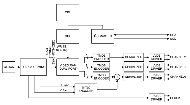
Figure 1. Functional block diagram of a DVI plug-in card.
DVI uses a 29-pin plug. Figure 2 and Table 1 show the pin configuration and assignment for DVI signals. The signal levels for LVDS channels are 0.5VP-P with a DC bias of 2.8V on both leads of each differential pair. The signal levels for the SDA and SCL pins allow levels up to 5V. The logic-high level on the hot-plug pin is greater than 2V.
Figure 2 displays the receptacle of the plug with all signals populated. Five different versions of plugs can be connected to this receptacle. Figure 3 shows the DVI-I (single link), DVI-I (dual link), DVI-D (single link), DVI-D (dual link), and DVI-A versions of the DVI plug. DVI-I, an acronym for DVI-Integrated, supports both digital and analog signals, so it works with both digital and analog monitors. DVI -D, an acronym for DVI-Digital, supports digital signals only. DVI-A, the acronym for DVI-Analog, supports analog signals only. 
Figure 2. DVI pin arrangement, receptacle.
Table 1. DVI Pin Assignment Pin Number Assignment 1 Data2- 2 Data2 + 3 Data2 / 4 Shield 4 Data4- 5 Data4 + 6 DDC Clock 7 DDC Data 8 Analog V Sync 9 Data1 + 10 Data1- 11 Data1 / 3 Shield 12 Data3- 13 Data3 + 14 + 5V 15 Ground 16 Hot-Plug Detect 17 Data0- 18 Data0 + 19 Data0 / 5 Shield 20 Data5- twenty one Data5 + twenty two Clock Shield twenty three Clock + twenty four Clock- C1 Analog Red Analog Green C3 Analog Blue C4 Analog V Sync C5 Analog Ground 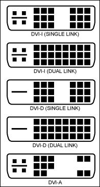
Figure 3. DVI pin arrangement, plug types.
Display Port (DP)
Figure 4 shows the functional block diagram of a DP architecture (dotted line) including the function of a GPU. This expanded GPU function has been integrated into most recent advanced CPU chipsets. The dedicated LVDS clock pair has been eliminated by using an embedded clock method . An 8B10B encoder is used instead of the TDMS encoder for lower EMI and enhanced embedded-clock recovery. A scrambler aids the clock recovery in case of idle signaling. Information bits are still coded in 8-bit format with the 8B10B encoder. The resolution is from 6 to 16 bits per color, which can be represented in either RGB or YCrCb format. The YCrCb is a digital version of YPrPb. Here, instead of dedicated channels for RGB signals, color information bits are distributed among four high-speed differential pairs according to their predefined maps. 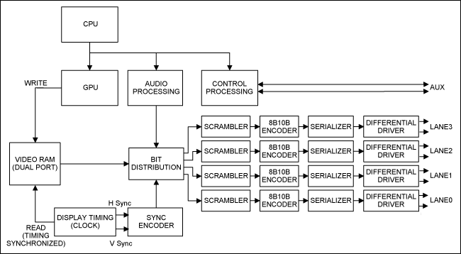
Figure 4. Functions of a DP-capable GPU.
High-speed differential channels are filled with data bits in sequences defined by control symbols such as BS (blank start) and BE (blank end). Control symbols are inserted into every high-speed differential channel. After BE, color pixel bits are equally distributed following the pixel sequence among all channels. For example, the distribution would be: pixel 0 for lane 0, pixel 1 for lane 1, pixel 2 for lane 2, pixel 3 for lane 3, pixel 4 for lane 0, etc. The BS is inserted after each line of pixels. Micropackets (VB-ID, MVID—video-stream time stamp, and Maud—audio-stream time stamp) are inserted on all lines after the BS. The VB-ID is used to identify some interlaced and audio features. Audio packets enclosed by the SS (secondary-data start) and SE (secondary-data end) can then follow. Filling bits framed by FS (fill start) and FE (fill end) can be used to fill the remaining empty time slots before the next BE symbol.
Instead of using an I²C format, control information is transmitted through a bidirectional auxiliary channel. The auxiliary channel is a differential pair using Manchester II encoding at a symbol rate of 1MHz. The differential voltage can range from 0.34V to 1.38V; the DC- bias voltage allows levels from 0V to the power supply of the differential device driver. The differential voltage is also AC coupled. The value of the AC-coupling capacitor can range from 0.075µF to 0.2µF. Native request and reply commands are defined for the auxiliary channel. I²C write and read transactions are mapped onto the auxiliary channel. The auxiliary channel can be used for several tasks: to get the desired extended display identification data (EDID) from a monitor; and to create a virtual control panel for monitoring the brightness, contrast, etc., controls with the monitor control command set (MCCS) protocol.
The DP has several uses: as an external interface to connect a PC to a monitor; as an internal interface to connect to the LCD display of a laptop; to connect consumer video electronics such as a DVD player with a flat-panel display. Because of the flexibility in the definition of these DP differential pairs, a GPU or graphics-capable CPU chipset can drive a DP-compatible monitor directly. Note that the DP does not preclude support of legacy signal types such as DVI or HDMI. In fact, GPUs or graphics-capable CPU chipsets provide the data processing capability to deliver additional DVI or HDMI signals. For GPUs and graphics-capable CPU chipsets without LVDS drivers, the MAX9406 can be used as a differential-signal level shifter, thereby allowing the implementation of DVI or HDMI interface formats.
The display port uses a 20-pin plug (Figure 5). Table 2 shows the pin assignment for all DP signals. The logic-high level for the hot-plug pin is greater than 2V. The DP power pin carries a voltage supply level of 3.3V. 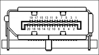
Figure 5. DP display port-pin arrangement.
Table 2. DP Display Port-Pin Assignment Pin Number Assignment 1 Lane0 + 2 Ground 3 Lane0- 4 Lane1 + 5 Ground 6 Lane1- 7 Lane2 + 8 Ground 9 Lane2- 10 Lane3 + 11 Ground 12 Lane3- 13 Ground 14 Ground 15 Aux + 16 Ground 17 Aux- 18 Hot Plug 19 Ground 20 DP_Power
MAX9406 HDMI / DVI Level Shifter 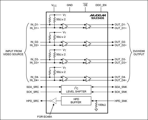
Figure 6. Functional block diagram of the MAX9406.
Figure 7 shows the MAX9406 in a typical application circuit with the DP. For this CPU chipset (Intel® Eagle Lake) implementation, lane 0 through lane 2 of the DP are mapped to channels 2 through 0 on the HDMI plug; lane 3 is mapped to the clock channel. Notice that signal parities are matched on corresponding channels. The auxiliary-plus signal is mapped to the SCL and the auxiliary-minus signal to the SDA. Proper software, often called chipset driver and video BIOS, needs to be installed to generate video signals corresponding to the HDMI protocol. The MAX9406 is only capable of high-speed and I²C-channel signal-level shifting. 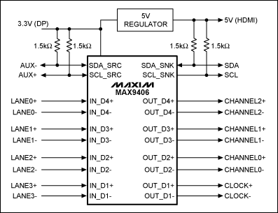
Figure 7. Typical application for the MAX9406.
The MAX9406 can be installed next to the GPU on the motherboard to enable an HDMI plug. The device can also be applied to a PCI Express® (PCIe®) plug-in card and plugged either into a bus slot (Figure 8) or a dongle board, which is plugged into a DP port (Figure 9). 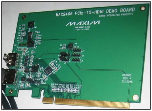
More detailed image (PDF, 765kB)
Figure 8. A MAX9406-based HDMI / DVI level-shifter plug-in card. 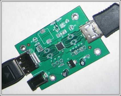
More detailed image (PDF, 3.35MB)
Figure 9. A MAX9406-based HDMI / DVI level dongle card.
HDMI is a trademark of HDMI Licensing, LLC.
Intel is a registered trademark of Intel Corporation.
PCIe is a registered trademark of PCI-SIG Corp.