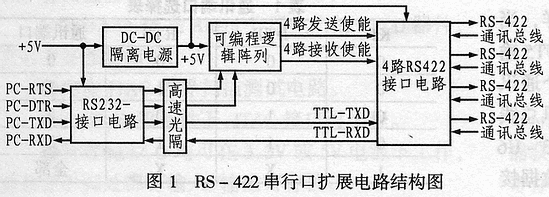
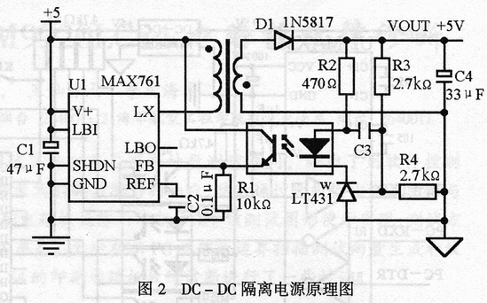
Abstract: This paper introduces the design method of serial port circuit which uses programmable logic array to expand 1 RS232 to 4 RS422. The expansion circuit does not occupy the resources of the PC system, and has the characteristics of simple structure, convenient use, versatility and compensability, and can be widely applied to the master-slave multi-machine communication system. Because the RS-422 bus has strong anti-interference ability, high communication speed, long communication distance, and communication with multiple slaves, the bus is master-slave multi-machine communication in data acquisition, monitoring management and distributed control system. It is widely used in the system. However, if too many slaves are connected to one RS-422 communication bus, the reliability of the system may be deteriorated due to excessive bus load, and sometimes the entire system may not work properly. In order to solve the problems that may occur in the practical application of RS422 bus, the author designed a serial port expansion circuit with programmable logic array GAL16V8 as the core. It can extend one RS232 serial port of the microcomputer to the 4-way RS-422 serial port. The circuit can program the DTR and RTS control signals through the host software, and can communicate with the slaves of the optional communication interface. It can also directly implement the slaves and all the communication interfaces between the slaves without DTR and RTS control signals. Data communication, while plug and play without changing the original software. In the actual gas leakage inspection system, the author uses the master-slave multi-machine communication network composed of the expansion circuit to realize the data communication between the host and more than 40 data acquisition devices, and ensures the communication performance is stable and reliable. Figure 1 shows the block diagram of this RS-422 serial port expansion circuit. The entire expansion circuit is divided into four parts, of which the first part is a DC-DC isolated power supply. In order to improve the anti-interference ability of the whole system, the circuit uses an isolated power supply for power supply. The second part is the RS-232 interface circuit, which is used to realize the RS-232 level and TTL level conversion of each signal. The third part is the RS485/RS422 interface circuit, which mainly realizes the RS485/RS422 level and TTL of each signal. The level conversion; the fourth part is the decoding control circuit with the programmable logic array GAL16V8 as the core, which is mainly used to realize the switching of the communication interface. 2.1 DC-DC isolated power supply In order to improve the anti-interference ability of the whole system, this circuit is powered by an isolated power supply. The working principle of the DC-DC isolated power supply is shown in Figure 2. The MAX761 DC-DC converter chip in the circuit operates in PFM (Pulse Frequency Modulation) mode with a maximum modulation frequency of 300kHz. The chip contains an error amplifier, a frequency modulator, and a power driver tube. The MAX761 requires only a few peripheral components to form a DC-DC power conversion circuit. The LT431 chip in the circuit is an open-collector error amplifier with a 2.5V reference. When the output voltage drops, the R4 voltage, error, LT431 output, optocoupler output current, and R1 voltage are all reduced. When the R1 voltage is less than the 1.5V reference voltage, the LX terminal outputs a low level during the positive half cycle of the modulation pulse. The pulse transformer initial current linearly increases, and D1 reverses the bias. At this time, the secondary pole has no current, and the pulse transformer starts. The energy is stored; and in the negative half of the modulation pulse, the LX terminal outputs a high level, the pulse transformer releases energy, and the induced voltage rises through the D1 (positive conduction) output to increase the output voltage. Thereby the output voltage remains stable. In fact, when the output voltage rises, the voltage and error on the R4 resistor, the output current of the LT431 output to the optocoupler, and the voltage on R1 rise accordingly. When the R1 voltage is greater than the 1.5V reference voltage, During the negative half cycle of the modulation pulse, the LX terminal outputs a high level, and the pulse transformer does not generate a voltage. At this time, the load consumption will cause the output voltage to drop. Thereby the output voltage remains stable. 2.2 RS-232 interface circuit The circuit connection of the serial port expansion circuit is shown in Figure 3. The MAX238 interface chip in the figure contains four RS-232 interface circuits, one of which is used for level conversion of RXD and TXD communication signals, and the other two are used for level conversion of DTR and RTS signals. The host software can set the status of DTR and RTS to select the communication interface, thereby realizing data communication between the host and the slave connected to the communication interface. The RS422/RS485 interface circuit consists of four (U3 ~ U6) MAX489 chips. The MAX489 chip contains a set of receive and transmit level shifting circuits. The chip is a full-duplex communication RS422 interface chip. The RE enable end (low active) on the chip is used to control data reception, and the DE enable end (high active) controls data transmission. In order to facilitate the debugging of the communication system, an illumination tube can be respectively installed at the receiving end, the transmitting end and each transmitting and transmitting end to observe the communication state of each channel. 2.4 decoding control circuit The U1 (GAL16V8) in the circuit is a programmable logic array that can be programmed to implement decode control. The communication port selection signals DTR and RTS sent by the host are input to U1 from IN5 and IN6, and the setting switch K1 is connected to U1 from IN1. Thus, when K1, DTR and RTS are decoded, they can be output from OUT1 to OUT5. The transmission enable terminals of U3~U6 respectively control the data transmitters of the four communication ports, thereby completing the data transmission of the host to the selected communication bus; and further, outputting the output enable terminals of U3 to U6 via OUT5~OUT8, The data receivers of the four communication ports can be separately controlled to finally enable the host to complete the receiving function of the slave data through the communication bus. The selection of its communication port is listed in Table 1. 3 Conclusion All the chips in the circuit are powered by a single +5V power supply, so the circuit structure is very simple. In addition, the circuit is powered by a DC-DC isolated power supply, and a high-speed optocoupler is used for optical isolation between the host and the communication interface, which also enhances the anti-jamming capability of the host system. The circuit has the characteristics of not occupying system resources, simple structure, convenient use, versatility and reliable performance, and can be widely applied to a master-slave multi-machine communication system with dual full-mechanism communication mode. 
The circuit is powered by a DC-DC isolated power supply, and a high-speed optocoupler is used between the host and the communication interface to achieve optical isolation, thereby enhancing the anti-interference capability of the host system. In addition, the expansion circuit has the characteristics of not occupying system resources, simple structure, convenient use, versatility and reliable performance, and therefore can be widely applied to a master-slave multi-machine communication system of full-duplex communication mode.
1 overall structure of the circuit
2 circuit working principle 
The DC-DC isolated power supply stabilizes the output voltage mainly by adjusting the frequency of the output pulse (adjusting the intermittent time of the pulse). The principle of the voltage regulation process is:
image 3
2.3 RS422/RS485 interface circuit
Table 1 Communication Port Selection Table K1 DTR RTS Communication port 0 0 0 0 0 0 1 1 0 1 0 2 0 1 1 3 1 X X All