PT62SCMD12 features: low jitter: 1ns typical; gate drive; overcurrent protection; dead time generator; undervoltage and overvoltage lockout PT62SCMD12 reference design application circuit: Figure 1PT62SCMD12 reference design The driver has an on-board dead-time generator which overrules the input signals when the deadtime of the applied PWM signals (tDEAD, IN) becomes larger than the set dead-time (tDEAD, PROG). Note that when the dead-time Generator has to intervene, the jitter increases to a maximum of 10ns. PT62SCMD12 Chinese data sheet: Click to download More schematics and source code popular application circuit: click now 8.4V Charger,8.4V Li-Ion Battery Charger,Battery Charger For Drone,Li Ion Battery Charger ShenZhen Yinghuiyuan Electronics Co.,Ltd , https://www.yhypoweradapter.com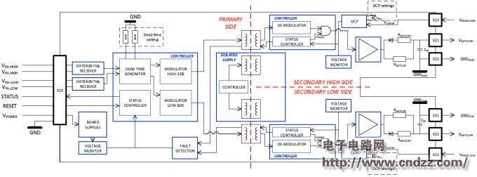
PT62SCMD12 Reference Design Circuit | MOSFET Driver Application Circuit
The PT62SCMD12 dual-channel silicon carbide MOSFET driver is designed by ProdriveTechnologies for the CAS300MxxBM2 module. This article mainly introduces the PT62SCMD12 features, application range, reference design circuit and circuit analysis to help you shorten the design time.