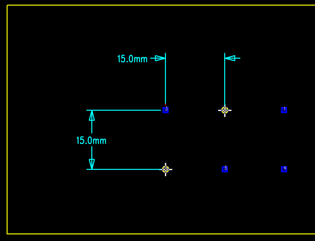
As a basic component of PCB surface mount assembly, and what is used to configure the pad pattern of the circuit board, the knowledge pool with a rich pad is indispensable as a good PCB engineer. According to the component manual drawing pad, many people will, but when drawing, pay attention to how to draw the best pad, I believe these tips will make you learn more complete pad knowledge. First, the type of pad In general, pads can be divided into 6 categories. 1. Square pads - printed circuit board components are large and small, and when printed conductors are simple. In the manual homemade PCB, using this kind of pad is easy to implement. 2. Circular pads - widely used in single and double sided printed boards where the components are regularly arranged. If the density of the board allows, the pad can be larger and does not fall off during soldering. 3. Island-shaped pad - the connection between the pad and the pad into one. It is often used in vertical irregular arrangements. For example, such pads are often used in tape recorders. 4. Teardrop pad—When the pad is connected, the trace is often used to prevent the pad from peeling and the trace is disconnected from the pad. This pad is often used in high frequency circuits. 5. Polygonal Pads - Used to distinguish between pads with different outside diameters and different apertures for easy processing and assembly. 6. Oval Pad - This pad has sufficient area to enhance the stripping resistance and is commonly used in dual in-line devices. Open-edged pad—used to ensure that the hole in a hand-welded pad is not blocked by solder after wave soldering. Second, the PCB design of the pad shape and size design standards 1. The unilateral minimum of all pads is not less than 0.25mm, and the maximum diameter of the entire pad is not more than 3 times of the device's aperture. 2. Should try to ensure that the spacing between the two pad edges is greater than 0.4mm. 3. In the case of dense wiring, it is recommended to use elliptical and oblong circular lands. The diameter or minimum width of a single-sided pad is 1.6mm; a double-faced weak circuit pad requires only a hole diameter of 0.5mm. If the pad is too large, it can easily cause unnecessary joint welding. The hole diameter exceeds 1.2mm or the pad diameter. Pads over 3.0mm should be designed as diamond or quincunx pads. 4. For plug-in components, in order to avoid copper foil breakage during soldering, the single-sided connection pad is completely coated with copper foil; however, the minimum requirement of the double-sided board is to make up for teardrops. 5. All the machine parts need to be designed as drip pads along the bending direction to ensure that the solder joints at the bent feet are full. 6. Pads on large area copper pads should use chrysanthemum solder pads instead of dummy solders. If the PCB has a large area of ​​ground and power line area (area over 500 mm2), it should be partially opened or designed as a grid fill. Pictured: Third, the PCB manufacturing process requirements of the pad 1. The test components shall be added at the two ends of the SMD component that are not connected to the inserted components. The diameter of the test point shall be equal to or greater than 1.8 mm to facilitate the test of the in-circuit tester. 2. The IC pad with a tight pitch is required to add a test pad if it is not connected to the hand-insertion pad. For a patch IC, the test point cannot be placed inside the patch IC's silk screen. The diameter of the test point is equal to or greater than 1.8 mm to facilitate in-line tester testing. 3. If the pad pitch is less than 0.4mm, white oil must be laid to reduce the over-peak soldering. 4. The tip and the end of the patch element should be designed with lead tin. The width of the lead tin is recommended to use 0.5mm wire, and the length is generally 2, 3mm. 5. If a single panel has a hand-welded component, it is necessary to open the tin bath. The direction is opposite to that of the tin. The width of the hole is 0.3mm to 1.0mm. 6. The spacing and size of the conductive rubber keys should be consistent with the actual size of the conductive rubber keys. The PCB board that is connected to this should be designed as a gold finger and the corresponding gold plating thickness should be specified. 7. The pad size and spacing should be exactly the same as the size of the patch component.
ZGAR Vape Pods 5.0
ZGAR electronic cigarette uses high-tech R&D, food grade disposable pod device and high-quality raw material. All package designs are Original IP. Our designer team is from Hong Kong. We have very high requirements for product quality, flavors taste and packaging design. The E-liquid is imported, materials are food grade, and assembly plant is medical-grade dust-free workshops.
From production to packaging, the whole system of tracking, efficient and orderly process, achieving daily efficient output. WEIKA pays attention to the details of each process control. The first class dust-free production workshop has passed the GMP food and drug production standard certification, ensuring quality and safety. We choose the products with a traceability system, which can not only effectively track and trace all kinds of data, but also ensure good product quality.
We offer best price, high quality Pods, Pods Touch Screen, Empty Pod System, Pod Vape, Disposable Pod device, E-cigar, Vape Pods to all over the world.
Much Better Vaping Experience!
ZGAR Vape 5.0 Pods,ZGAR Vape Pods 5.0,ZGAR Vape Pods 5.0 Pod System Vape,ZGAR Vape Pods 5.0 Disposable Pod Vape Systems ZGAR INTERNATIONAL(HK)CO., LIMITED , https://www.zgarvapor.com

