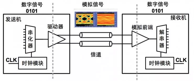
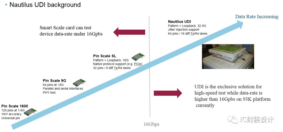
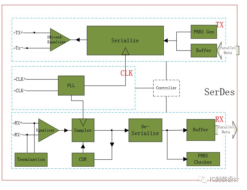
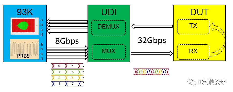
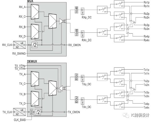
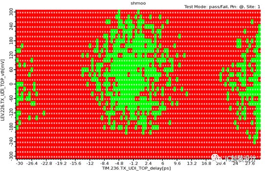
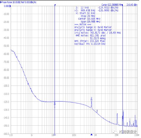
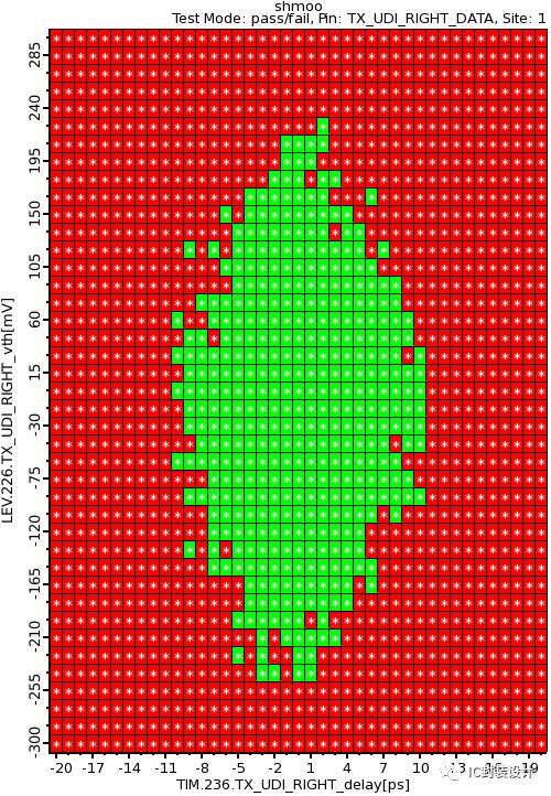
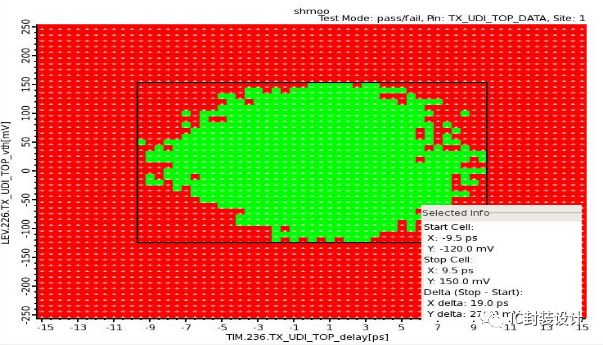
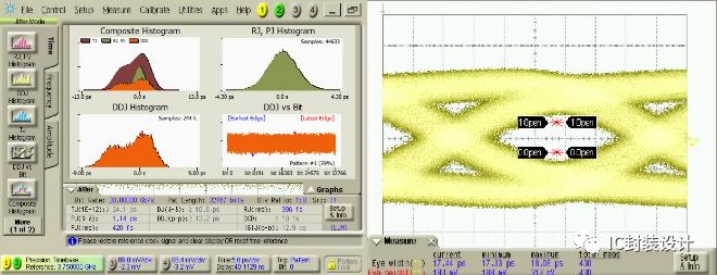
With the continuous increase of the degree of integration, complexity, and transmission rate of the SerDes chip, the traditional automated test system has been unable to meet the SerDes test rate requirements. However, with the introduction of the Nautilus UDI solution, mass production testing of 32 Gbps SerDes was successfully performed. So, how does the Nautilus UDI solution implement high-speed SerDes testing including UDI architecture, input clock design, Load board design, and socket selection? introduction With the development of information and communication technologies, the rate and efficiency of data transmission are increasingly demanding, and the speed of traditional parallel interfaces has reached a bottleneck. The faster serial interfaces are the trend of technology development. The SerDes technology originally used for optical fiber communications became the mainstream of high-speed serial interfaces. SerDes automated testing is subject to the test system transmission rate limit and hardware design, resulting in SerDes testing far behind the development of SerDes chips. After years of research and development and high-speed IO testing experience, Advantest has developed a complete set of high-speed support up to 32.8 Gbps (Nautilus UDI) based on the 93000 platform, which complements the 16G-32.8 Gbps SERDES high-speed IO automation test. Whitespace. Figure 1: The 93000 platform provides SerDes test solutions that support a wide range of transmission rates, including 9 Gbps, 16 Gbps, and 32.8 Gbps. Figure 1: 93000 0-32G Transmission Rate Test Plan 1 SerDes SerDes is an abbreviation of English Serialize/De-Serialize. It is a mainstream time-division multiplexing (TDM), point-to-point (P2P) serial communication technology. That is, the multi-path low-speed parallel signal at the transmitting end is converted into a high-speed serial signal, passes through the transmission medium (optical cable or copper wire), and finally the high-speed serial signal at the receiving end is converted back to a low-speed parallel signal [1]. The PCIE, SATA, and other interfaces in common consumer electronics products are examples of SerDes technology applications. SerDes mainly consists of PLL clock module, control module, transmitter and receiver (as shown in Figure 2). In order to solve test problems and reduce test costs, today's SerDes also adds pseudo-random code (PRBS) generators, pseudo-random code (PRBS) checkers, and loop-back paths and other module-assisted tests. Figure 2: SerDes structure 2 SerDes test The SerDes test is mainly divided into BIST tests and high speed I/O tests. The BIST test mainly relies on the internal test module of the chip, and the test chip function is normal. The main features of the BIST test are high test efficiency, low cost, low requirements for hardware production such as load board, but it cannot test the characteristics of the chip, and the test coverage is relatively low. , and cannot fail to locate. The High speed I/O test can basically meet all SerDes test requirements. The test coverage is high, but it has high requirements for hardware production and high test costs. SerDes High speed I/O based test module can be divided into two parts: receiver test and transmitter test. Receiver performance indicators include: sensitivity test, jitter tolerance test, skew test, impedance test, etc. Transmitter performance indicators are: output amplitude test, eye height, eye width test, rise and fall time test, jitter test (TJ, RJ/DJ), eye diagram test, common mode voltage test, skew test, impedance test, etc. [2 ]. 3 Nautilus UDI solution The Nautilus UDI (abbreviated as UDI below) scheme is shown in Figure 3. The 93000 sends 4 8 Gbps signals to UDI, and the UDI internal MUX synthesizes a 32 Gbps signal to the chip. The receiver is combined with a chip-based pseudo random code checker. test. The internal transmitter of the chip transmits 32 Gbps signals, and after being decomposed into four 8-bit Gbps signals through the DEMUX, the 93000 samples are tested and analyzed, and the transmitter test is realized. With the parallel parallel back model of the chip [3], we usually cover the receiver and transmitter with loop-back eye diagram test in actual production. The UDI test rate is 16G~32.8 Gbps (up to 64 Gbps in the future) and can support up to 16 receiver and transmitter tests. Figure 3: UDI Test Plan Model 3.1 How Nautilus UDI Works UDI is mainly composed of MUX and DEMUX 2 circuits. The MUX incorporates a 4:1 multiplexer (as shown in Figure 4). The first 2:1 multiplexer is controlled by an RX_CLK (4 Ghz) x2 clock to achieve AC, BD synthesis, X4 times The frequency clock controls the second-level 2:1 multiplexer and converts it to ABCD. Then through an output amplitude (0 ~ 1200mV) adjustable amplifier and 10db attenuator as an output (0 ~ 260mV), to meet the test receiver sensitivity function and accuracy requirements. In addition to providing the mux trigger clock, RX_CLK adds jitter to the output signal by adding jitter to RX_CLK to achieve the purpose of measuring receiver tolerance. DEMUX structure and MUX approximation, built-in a 1:4 multi-way demultiplexer, and a passive equalizer before the DEMUX, so that the distortion caused by the path insertion loss signal is more flat, reducing the code caused by the path Interference. Figure 4: MUX and DEMUX structures 3.2 chip input clock SerDes has a higher requirement for the reference clock. The RJ of the input clock is mixed by SerDes and cannot be used to test the true jitter of the chip. As shown in Figure 5, a reference clock with RJ=1ps is used (SerDes requires RJ<400fs). Too many points do not guarantee test stability. For this purpose, we have selected a standardized module, the Jitter Attenuator Module (JAM for short), and programmable control it through the 93000 to achieve different frequency clock input noise reduction processing. After the JAM, the reference clock RJ is reduced to within 300 fs (see Figure 6). There is no scatter in the scanned eye diagram (Figure 7), which ensures the stability of the mass production test. Figure 5: RJ=1ps system clock, PLB eye diagram Figure 6: JAM Output Clock Phase Noise Index Figure 7: PLB Eye Diagram Using JAM as Reference Clock 3.3 Load Board Design The SerDes high-speed IO interface test requires high signal integrity for the transmit and receive pin peripheral circuits. A slight carelessness can result in large errors in the test results. For the SI rules we propose the following points: 1) For TX, the TDR requirement for the RX full-link (including vias) is a single-ended impedance of 50 Ω ± 5 Ω and a differential impedance of 100 Ω ± 10 Ω. 2) The packaging factor needs to be taken into consideration, and the equal attenuation between lanes is used instead of the equal length of the line that originally considered only the load board. 3) For Load Board materials, use materials with a small dielectric constant, such as Roger, Megtron6, and Necole. The smaller the dielectric constant, the smaller the line loss attenuation [4]. 4) The requirements for high-speed cabling for full-links (linewidth, spacing must be sufficient, signal packet processing, etc.). 5) After the Load board design is completed, "3D" simulation must be used to meet the requirements of S21>-3db@15GHz; S21>-6db@30GHz. 3.4 Socket selection Socket is also an important part of the test, mainly pogo pin and conductive adhesive 2 kinds of materials, Pogo pin socket durability, high and low temperature difference is not suitable for mass production use. Conductive plastic sockets have low signal attenuation due to processing characteristics and are suitable for high-frequency testing. However, because they are not wear-resistant and cannot meet the requirements for mass production, they are only suitable for characteristic tests. 4 test results Using the UDI solution We performed a PRBS15 loopback test on a 32 Gbps SerDes chip. The eye widths of the UDI test were 19 ps and 270 mV (Figure 8), which are basically consistent with the DCA measurement results (Figure 9). Figure 8: UDI Eye Diagram SHMOO Scan Figure 9: DCA Measurement Results 5 Conclusion The Nautilus UDI solution provides a complete solution for high-speed I/O interface feature testing and mass production test automation. Once it was launched, it was recognized by many domestic and foreign customers, and it cooperated with a well-known domestic semiconductor company to realize multiple 25- The stable mass production of 32G Bps SerDes chips is expected to help solve the problem of high-speed I/O testing in the future for customers still suffering from high-speed SerDes testing. Hall Voltage Sensor,Hall Effect Voltage Sensor,Open Loop Voltage Sensor,Open Loop Hall Voltage Sensor Zibo Tongyue Electronics Co., Ltd , https://www.tongyueelectron.com