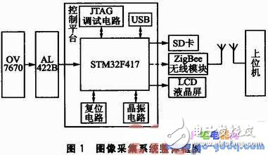
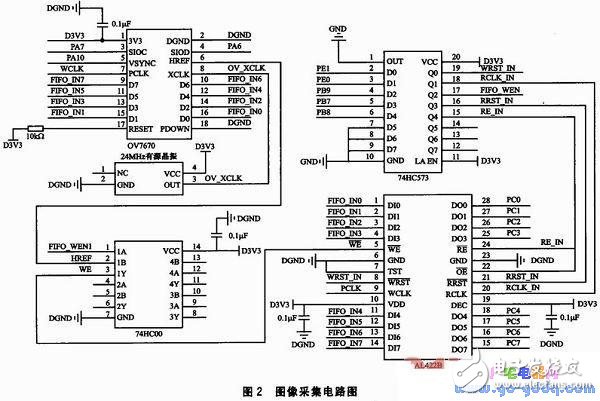
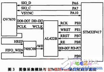
Video image acquisition and processing systems are widely used in industrial control, industrial inspection, medicine, machine vision and other fields, and video communication is an important part of multimedia applications in the 3G era. Digital cameras, video phones, conference calls, etc. seen in daily life. Products, real-time image acquisition is its core technology. The speed and quality of image acquisition directly affect the overall effect of the product. Most embedded image acquisition systems are based on DSP and ARM technology. Some systems are complex, costly, and difficult to process in real time. The image acquisition system based on STM32F417 designed in this paper has the advantages of lossless image quality, good real-time performance, low power consumption and low cost. It is suitable for applications in systems with high requirements for real-time information and image quality. The image acquisition system is mainly composed of STM32F417 microprocessor, CMOS camera, frame buffer, SD card, LCD screen and other peripherals. The overall block diagram of the image acquisition system is shown in Figure 1. 1.1 Core Microcontroller Embedded microprocessors are the best choice for portable systems due to their high performance and low power consumption. The STM32F417 developed by ST is a 32-bit flash microcontroller based on the ARM Cortex-M4 core. Its main frequency is 168 MHz, its processing performance can reach 210 MIPS at this operating frequency, and the current consumption is only 38.6 mA; it supports multiple low-power modes of operation; internal integrated DSP and FPU instructions, high performance Signal processing and floating point computing capabilities; with an 8 to 14-bit parallel camera interface. In addition, the STM32F417 integrates 1 MB of Flash and 196 KB of SRAM on-chip. Using STM32F417 as the control core of the image acquisition system will greatly improve system performance and reduce power consumption and cost. 1.2 CMOS camera The CMOS camera uses OmniVision's OV7670. It is embedded with a 10-bit A/D converter, which can output image data in 8-bit RGB/YCbCr/YUV format. The maximum frame rate is up to 30 frames/s, the maximum image resolution is 640 & TImes; 480, and the power supply voltage is 3. 3 V. The O7670 comes with a standard SCCB bus interface and is compatible with the I2C bus interface. 1.3 frame buffer The large-capacity AL422B of American AverlogIC Technologies was selected as the shared data RAM for sampling processing. It is a FIFO memory chip with a storage capacity of 384 K&TImes; 8 B and operates at up to 50 MHz. All addressing, refreshing, etc. operations are performed by a control system integrated inside the chip. In this design, one frame of image data contains 320 & TImes; 240 pixels, and a full frame of image storage requires 153 600 bytes. The capacity of AL422B fully meets the design requirements of the system. 1.4 SD card The SD card is a new generation of memory devices based on semiconductor flash memory and has a wide range of applications. This design uses Kingston 8 G SD memory card to store the collection information, which is convenient for the system to further process the information. 1.5 LCD screen and other peripherals The LCD screen uses a 3.2-inch TFT LCD screen 320QVT with a resolution of 240 & TImes; 320, and its data pin is directly connected to the FSMC bus interface. Other peripherals include LCD interface circuits, ZigBe e wireless modules, JTAG debug circuits, reset circuits, crystal oscillator circuits, and more. 1.6 Image acquisition circuit design The camera image acquisition circuit uses a 24 MHz active crystal to provide the system clock for the OV7670. In order to solve the problem of inconsistent data transmission rate between the microprocessor and the camera, an AL422B frame buffer is added between the two, and the image data collected by the camera is buffered and then sent to the microprocessor. In order to automatically store the image signal output by the OV7670 into the AL422B chip, the circuit uses a NAND gate chip 74HC00 to generate a write timing that meets the requirements of AL422B. It should be noted that since the AL422B chip needs 3.3 V power supply for normal operation, if the STM32 F417 is powered by 3 V, a 74HC573 D latch needs to be added between the two chip interfaces to meet the high/low level. Claim. The image acquisition circuit diagram is shown in Figure 2. The interface circuit diagram of the image acquisition module and STM32F417 is shown in Figure 3. In FIG. 3, the PC0 to PC7 ports of the STM32F417 are used to receive the 8-bit image data output by the OV7670 after being buffered by the AL422B. The SIO_D and SIO_C interfaces of the OV7670 are connected to the PA6 and PA7 pins of the STM32F417, and the initial configuration of the camera is realized through this interface. PE0, PE1, PB7, and PB8 of STM32F417 control the clock signal, write reset, read reset, and read enable signal of AL422B, respectively. The PB9 and OV7670 output line scan signals are controlled by the non-chip implementation of the frame buffer write enable. The PA10 pin of the STM32F417 detects whether the camera outputs a complete image by interrupt. Because the OV7670 has a standard SCCB interface and is compatible with the I2C bus interface, this design uses the I2C bus signal generated by the STM32F417 to simulate SCCB, which realizes the initial configuration of the internal register of the camera and the setting of its line sync signal, window opening and output format. The configuration method of the OV7670 register is as follows: First, the write address 0x42 of the OV7670 is sent, and then the destination register address and data of the write data are sent, thereby initializing the write operation; by transmitting the read address 0x43 of the OV7670, the initialization of the read operation is completed, thereby realizing Initial configuration of the OV7670 camera. During the configuration of the camera operating parameters, the register DBLV of the OV7670 is set to 0x80 to control the input clock multiplier. Set the registers BRIGHT, CONTRAS to control the brightness and contrast of the image. The upper and lower limits of the image edge enhancement are set by the registers REG75 and REG76. In the camera test phase, first set the register ACALING_YSC to 0x85, display 8 color bars, and set the register to 0x00 after the test phase to enter the non-test mode. The OV7670 output sync signal includes: field sync signal VSYNC, line sync signal HREF, and pixel clock PCLK. According to the synchronization signal timing diagram provided in the OV7670 data sheet, the pixel clock PCLK of the OV76 70 camera is connected to the FIFO write clock WCLK, and the data is written to the FIFO when PCLK is active. The field sync signal VSYNC scans one frame of image timing and completes scanning of one frame of image between two positive pulses. When the STM32F417 detects the falling edge of VSYNC for the first time, the system generates an interrupt for the first time, indicating that the OV7670 starts to output one frame of image, STM32F417 sets FIFO_WEN high, and when HREF is active (high), FIFO_WEN and HREF pass The WCK of the NOT gate enable FIFO automatically writes valid image data into the FIFO. When the second VSYNC interrupt is generated, it indicates that a complete frame of image has been written into the FIFO. The system latches one frame of image data by setting FIFO_WEN low to achieve static storage of the image. At this time, STM32F417 sends a rising edge to the read clock RCLK of the FIFO, and reads the data from the FIFO to complete the real-time acquisition and extraction of image data. 1.7 storage module The SD card supports both SPI and SD modes. This design uses SPI mode to connect the CMD pin of the SD card to the SPI3_MOSI of the SFM32F417, CLK to the SPI3_SCK pin of the STM32F417, DATA0 to the SPI3_MISO pin of the STM32F417, and DATA3 as the chip select CS. Connected to the PA15 of the STM32F417; when the SD card receives the reset command, if the CS is active, the SPI mode is started, and the SD card reads and writes data through DATA0 under the control of SPI3_SCK. A business tablet must have powerful business functions. At present, users use tablet products more for entertainment, and insufficient development of commercial value has become a major factor restricting the development of tablet computers. Many far-sighted terminal manufacturers have set their sights on the business tablet field. Business Tablet,4k Tablet,5G Tablet Jingjiang Gisen Technology Co.,Ltd , https://www.gisentech.com


Generally speaking, when business users choose tablet PC products, they still focus on "regular items" such as processor, battery, operating system, and built-in applications, especially office software applications, which are a good helper for business users.
First of all, there must be powerful office software such as customer management software, which can record customer data and related information anytime, anywhere. There is also a need for powerful marketing software, software marketing, reducing manual intervention, and one person can handle all the publicity and customer information.