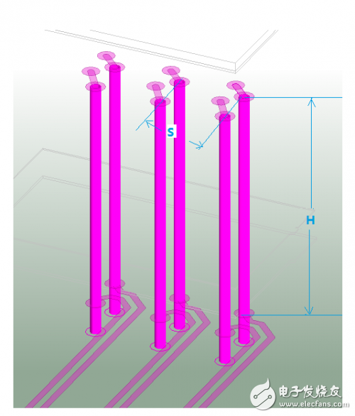
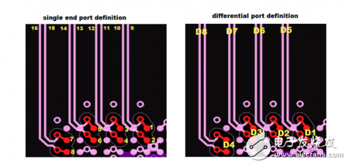
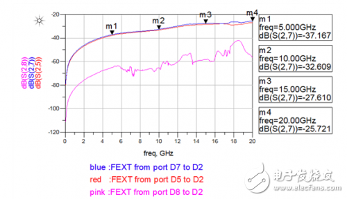
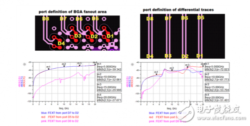
In hardware system design, the crosstalk we usually focus on mainly occurs between connectors, chip packages, and parallel traces with close spacing. However, in some designs, large crosstalk is also generated between high-speed differential vias. This paper provides an example simulation analysis and solution for the crosstalk between high-speed differential vias. For thicker PCBs, the thickness may be 2.4mm or 3mm. Take a 3mm board as an example. At this time, the length of a through hole on the PCB in the Z direction can reach nearly 118mil. If there is a 0.8mm pitch BGA on the PCB, the fan-out via spacing of the BGA device is only about 31.5 mils. As shown in FIG. 1, the parallel length H of the two pairs of adjacent differential vias in the Z direction is greater than 100 mils, and the spacing of the two pairs of differential vias in the horizontal direction is S = 31.5 mils. When the parallel distance of the Z direction between the via holes is much larger than the horizontal direction, the crosstalk problem between the high speed signal differential vias is considered. By the way, high-speed PCB design should minimize the length of the via stub to minimize the impact on the signal. As shown in the figure below, the Stub will be shorter than the Bottom layer. Or you can use the way of back drilling. Figure 1: High-speed differential vias for crosstalk (H>100mil, S=31.5mil) The following is a simulation of a design example with a plate thickness of 3 mm, a 0.8 mm BGA fan-out pitch pitch of 31.5 mils, and a via parallel distance H=112 mil. As shown in Figure 2, we define 4 pairs of differential pairs into 8 differential ports based on the traces. Figure 2: Crosstalk simulation port definition Assuming that the differential ports D1 - D4 are the receiving ends of the chip, we analyze the crosstalk of adjacent channels by observing the far-end crosstalk of the D2 ports on the D5, D7, and D8 ports. From the results shown in Figure 3, we can see two channels that are close together. The far-end crosstalk between channels can reach -37dB@5GHz and -32dB@10GHz, and further optimization is needed to reduce crosstalk. Figure 3: Crosstalk simulation results between differential pairs Perhaps you will have questions when reading this: How do you determine crosstalk caused by differential vias instead of crosstalk caused by differential traces? To illustrate this problem, we divide the above example into two parts: the BGA fan-out area and the differential trace. The simulation results are shown in Figure 4: Figure 4: BGA fan-out area and differential trace crosstalk simulation results From the simulation results on the right side of Figure 4, it can be seen that the crosstalk between the differential traces is below -50dB, and even below -60dB in the 10GHz band. The crosstalk of the BGA fan-out area is close to the crosstalk value of the original overall simulation. From the simulation results in Fig. 4, we can conclude that the crosstalk between the differential vias plays a major role in the above example. SUNLUX IOT Technology (Guangdong) INC. , http://www.sunluxbarcodereader.com


