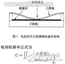
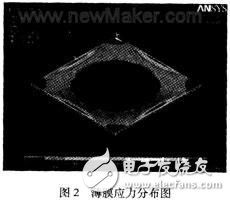
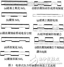
The basic structure of the capacitive pressure sensor is shown in Figure 1. Where: ε0 is the dielectric constant in vacuum; t is the thickness of the insulating layer; εr is the relative dielectric constant of the insulating layer; g is the initial distance between the two plates of the capacitor at zero load; ω(x, y) is The vertical displacement of the midplane of the plate film. It can be seen from the formula that the external pressure changes the capacitance by changing the plate area and spacing of the capacitor. As the pressure increases slowly, the capacitance increases due to the decrease in the distance between the plates. At this time, the capacitance value is determined by the non-contact capacitance; when the two plates are in contact, the size of the capacitance is mainly determined by the contact capacitance. The sensitive film is the core component of the sensor, and its material, size and thickness determine the performance of the sensor. At present, materials for sensitive films are mostly heavily doped with p-type silicon, Si3N4, single crystal silicon, and the like. Each of these materials has its own advantages and disadvantages, and its choice is related to the target requirements and specific processes. The silicon film does not damage the crystal lattice, has excellent mechanical properties, and is suitable for anodic bonding to form a cavity. From the purpose of simplifying the process, the silicon film is selected in the present scheme. The working state of the film of the contact structure was simulated by the finite element analysis software ANSYS. The material is Si, the shape of the film is square, the side length is 1000 μm, the film thickness is 5 μm, and the plate spacing is 10 μm. Under the atmospheric pressure of 1.01 & TImes; 105Pa, the central contact portion and the four corners of the film are basically unstressed, and the central stress on the four sides is 1.07 MPa at the maximum, which is less than 7 MPa, and the stress distribution is as shown in Fig. 2. The entire manufacturing process uses a standard process, as shown in Figure 3. The SiO2 of 100 nm is thermally oxidized first, both as a mask for etching Si and as an insulating layer for the two electrodes of the capacitor. The anisotropic etching is used to form the capacitor cavity and the stop groove of the future dew electrode. If the thickness of the silicon wafer is uniform and the KOH corrosion rate is uniform, the method can be equivalent to self-stop corrosion to a considerable extent. The two electrodes of the capacitor are taken out from the glass and then anodically bonded to the silicon wafer. The bonding sheet is thinned by KOH etching and then subjected to deep etching of the reactive ions to expose the measuring electrode. Steel Crossarm,Steel Cross Arm,Steel Cross Brace,Galvanized Steel Cross Arm Jiangsu Baojuhe Science and Technology Co.,Ltd. , https://www.galvanizedsteelpole.com


Basic principle and structural design of MEMS silicon film capacitive pressure sensor
Basic principle and structure